
Electronics Unit 4: Digital Logic, Microcontrollers and Applications
Subject: Fundamentals of Electronics Engineering
University: AKTU
Course: B.Tech First Year
Semester: I & II
Course Codes: AEC101A / AEC201A | AEC101B / AEC201B | AEC101C / AEC201C
Applicable Streams: CSE, EE, ECE, CE, ME, CH, TX, BT & AG
Unit IV Introduction
Digital electronics represents information with defined logic states. This unit connects number systems, gates, Boolean simplification and storage to microcontroller acquisition, industrial decisions, displays and agriculture/biomedical readout.
Topics Covered
| Topic | Pages |
|---|---|
| Number systems and conversions | 3–7 |
| Levels, gates and Boolean laws | 7–12 |
| K-maps and minimisation | 12–17 |
| Adders, ALU and multiplexers | 17–23 |
| Storage, GPIO and PLA/PLD | 23–27 |
| ADC, controller and displays | 27–30 |
| Industrial and BT/AG applications | 30–34 |
| Formulae and quick revision | 34–35 |
Coverage
All six A/B/C course codes and nine streams. The branch-wise topic guide identifies the prescribed sections. Read the shared foundation, then follow your prescribed application sections.
How to Use These Notes
- Start with the branch/topic guide.
- Declare variable order and the meaning of each input.
- Check all truth-table rows after simplification.
- Use Gray order and valid groups in each K-map.
- Separate present logic, stored state and clock events.
- Trace raw code to units, decision and output driver.
What Is Included?
| Study Support | Included |
|---|---|
| Worked problems | 50 numbered problems with steps and checks. |
| Labelled figures | Gate circuits, K-maps, storage and application paths. |
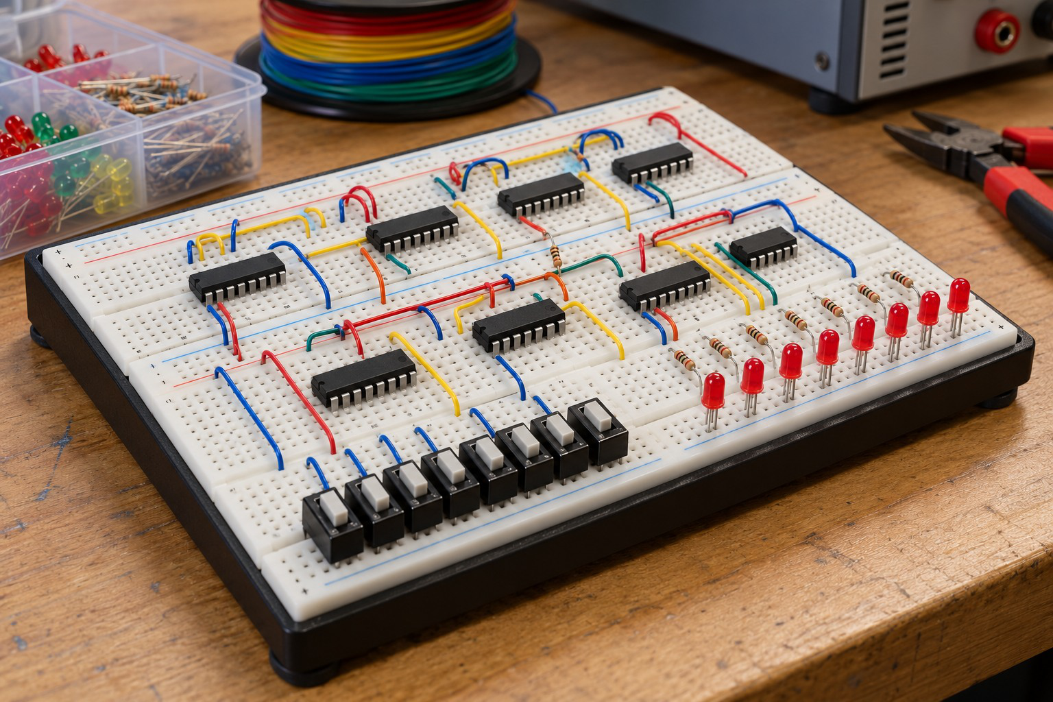
| Realistic images | 10 component and application photographs. |
| Dedicated applications | ALU/routing, industrial control, sensor readout, irrigation and data logging. |
| Revision | Formula conditions, memory cues and short answers. |
Key Distinction
Boolean + means OR; arithmetic + means numerical addition. A carry bit has weight two in a one-bit adder. State which operation is intended before manipulating an expression.
Numerical Convention
Values are educational assumptions. Retain precision until the final answer. An approximate model is valid only within its stated conditions.
Unit Overview and Branch-Wise Reading Map
Select your prescribed topics using this guide. The A group develops digital logic in detail; B and C share logic levels, selected gates and acquisition/display concepts, then follow their dedicated applications. Extra logic detail remains optional enrichment for B/C.
| Topics / Application Block | Applicable Branches | Where to Read |
|---|---|---|
| Binary, decimal, hexadecimal and conversions | A: CSE, EE, ECE | Sections 1–7 |
| Logic levels, digital signals, AND / OR / NOT; GPIO principles | All nine streams | Sections 1, 8–9, 33, 36 |
| NAND truth table and simple industrial Boolean rule | B: CE, ME, CH, TX | Sections 9, 38 |
| NAND/NOR/XOR, Boolean laws, De Morgan and K-maps up to 4 variables | A: CSE, EE, ECE | Sections 9–21 |
| Half/full adders, ALU, MUX, SR/D storage and PLA/PLD | A: CSE, EE, ECE | Sections 22–34 |
| ADC concept, microcontroller input/decision/output, LCD and seven-segment | B: CE, ME, CH, TX; C: BT, AG | Sections 35–37 |
| Plant temperature/pressure readout, ON/OFF and PLC ladder concept | B: CE, ME, CH, TX | Sections 38–39 |
| Soil moisture/pump, thermometer, fermentation pH, logging, pulse-oximeter display | C: BT, AG | Sections 40–43 |
| Formulae, model checks and quick revision | All: select relevant topics | Section 44 |
Syllabus Groups and Official Unit Names
- A — CSE, EE, ECE: Digital Electronics Basics.
- B — CE, ME, CH, TX: Digital Basics and Microcontroller Overview.
- C — BT, AG: Digital Basics and Microcontroller in BT/AG.
What Is Included
50 numbered solved problems, 10 realistic component/laboratory images, labelled gate circuits, maps and application illustrations. Both semester codes within each group have the same unit syllabus. Gate truth tables distinguish the narrower B/C requirements from A-only logic lessons.
Reading rule: Define inputs, derive the required output and verify the model. A Boolean command, voltage level, ADC code and displayed physical value are different quantities. Numerical examples use explicitly stated assumptions.
1. Digital Information and Notation
Digital electronics represents information by a finite set of states. Binary circuits use two logical values, 0 and 1, represented physically by specified voltage ranges. A bit is one binary digit. A group of bits can describe an unsigned number, an instruction, a character or a control condition; the interpretation comes from the system.
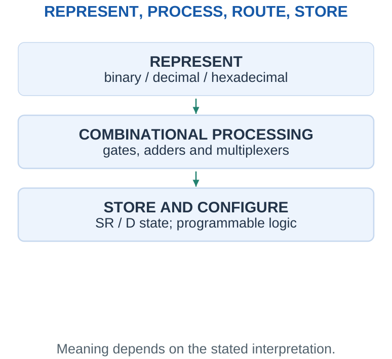
Conventions used in this unit: Positive logic associates HIGH with 1 and LOW with 0. A prime means NOT: A’ is the complement of A. Adjacent letters or a dot mean AND; + means Boolean OR; ⊕ means XOR. Boolean OR is different from arithmetic addition: 1 + 1 = 1 in Boolean algebra, but adding two binary ones arithmetically produces 10.
Number-system examples use an explicit base in words or a subscript. Unless a question says otherwise, numbers are nonnegative integers and binary words are unsigned. Fractional conversion and signed representations are outside the core conversion requirement here.
Start correctly: Write the base and bit width where relevant. The written digits 10 mean two in binary, ten in decimal and sixteen in hexadecimal.
2. Binary Place Values and Decimal Value
A positional number system gives each position a power of the base. Decimal uses powers of ten; binary uses powers of two. The rightmost integer bit has weight 2^0 = 1. Moving left doubles the weight: 1, 2, 4, 8, 16, 32, 64, 128 and so on.
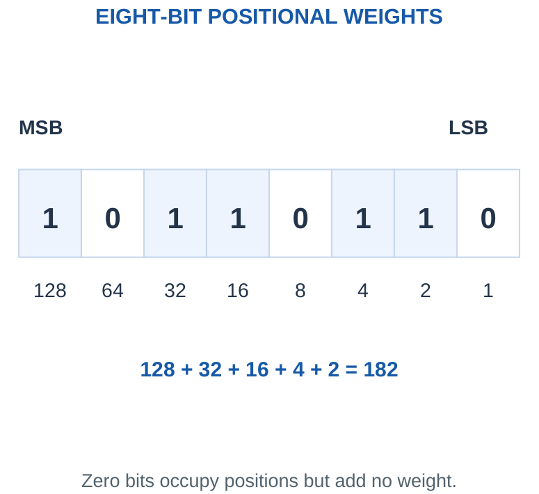
For binary b7b6…b0, decimal value is b7 × 128 + b6 × 64 + … + b0 × 1. The most significant bit (MSB) is the highest-weight bit of the specified word; the least significant bit (LSB) has weight one. Leading zeros preserve value but can communicate a required width.
A four-bit group is a nibble and an eight-bit group is a byte. Bit count and numerical value are different quantities: 10000000 has eight bits but unsigned decimal value 128. The largest eight-bit unsigned value is 11111111, which equals 255.
Fast check: An integer is odd exactly when its binary LSB is 1. This is a useful error check, not a substitute for the complete weighted sum.
Worked Problem 4.1: Read Binary Weights
Problem: Convert binary 101101 to decimal using positional weights. Interpret it as unsigned.
Model / approach: The rightmost bit has weight one; count every position including zeros.
Step 1: The 1 positions contribute 1 + 4 + 8 + 32.
Step 2: Adding those weights gives 45.
Answer: (101101)₂ = (45)₁₀.
Check and interpretation: The word contains 6 bits, so its value must be at most 63. The final bit also confirms whether the value is odd or even. Leading zeros would change the written width without changing this value.
3. Decimal-to-Binary Conversion
For a nonnegative integer, repeatedly divide by two, recording each remainder. Stop when the quotient becomes zero. Read the remainders from the last division back to the first. The first remainder obtained is the LSB, not the MSB.
Alternative: descending weights: Choose the largest power of two not exceeding the number. Write 1 at that weight, subtract it and continue through every lower weight, writing 0 where a weight is not used. This method and repeated division must give the same result.
Always verify by converting the final binary word back to decimal. For zero, write 0 or the all-zero word of the requested width. If the result needs fewer bits than a specified word, pad with leading zeros. If it needs more bits, state that it does not fit; do not silently discard the leftmost digits.
Memory trick: Divide down, read up. A reversed remainder sequence is one of the most common conversion errors.
Worked Problem 4.2: Repeated Division by Two
Problem: Convert decimal 37 to binary and write the result as an eight-bit unsigned word.
Model / approach: Divide repeatedly; read the recorded remainders upward.
Step 1:
- 37 ÷ 2 = 18, remainder 1
- 18 ÷ 2 = 9, remainder 0
- 9 ÷ 2 = 4, remainder 1
- 4 ÷ 2 = 2, remainder 0
- 2 ÷ 2 = 1, remainder 0
- 1 ÷ 2 = 0, remainder 1
Step 2: Reading upward gives 100101. Pad to eight bits: 00100101.
Answer: (37)₁₀ = (00100101)₂.
Check and interpretation: Converting back gives 37. It fits because 37 ≤ 255. Remainders in their original downward order would generally encode a different value.
4. Binary-to-Decimal Conversion and Checking
Multiply each bit by its positional weight and add the contributions. Zero bits contribute nothing but still occupy positions. Losing an internal zero shifts later weights and changes the value.
A second method: multiply and add: Scan from the left. Start at zero and repeatedly calculate new value = 2 × old value + next bit. For 1011: 0 → 1 → 2 → 5 → 11. This method is particularly useful for checking a long weighted-sum calculation without writing all powers separately.
Worked check: Leading zeros versus shifted zeros
Binary 001101 has decimal value 13, just like 1101. Binary 110100 instead equals 52 because two zeros appended on the right multiply an unsigned integer by four. Leading padding preserves value; trailing zeros generally change it. Distinguish padding for width from shifting a value.
An n-bit unsigned word lies from 0 through 2^n – 1. A result outside that interval cannot be the value of that word. The number of possible words is 2^n, which is one more than the maximum value because zero is included.
Avoid ambiguity: The binary word 1111 is decimal 15 in the unsigned convention used here. A signed interpretation needs an explicitly defined representation; it should not be introduced into an unsigned conversion question.
5. Hexadecimal Digits and Decimal Conversion
Hexadecimal is base sixteen. Its digits are 0–9 and A–F, where A = 10, B = 11, C = 12, D = 13, E = 14 and F = 15. Each position has weight 16^k. For example, 2F means 2 × 16 + 15 = 47 in decimal.
Worked check: Keep an internal zero nibble
Hexadecimal A03 expands to 1010 0000 0011. It is decimal 2563. Removing the middle zero nibble gives A3, decimal 163, which is a different value. Only leading zeros may be omitted without changing an unsigned integer; zeros inside the word preserve positional weights.
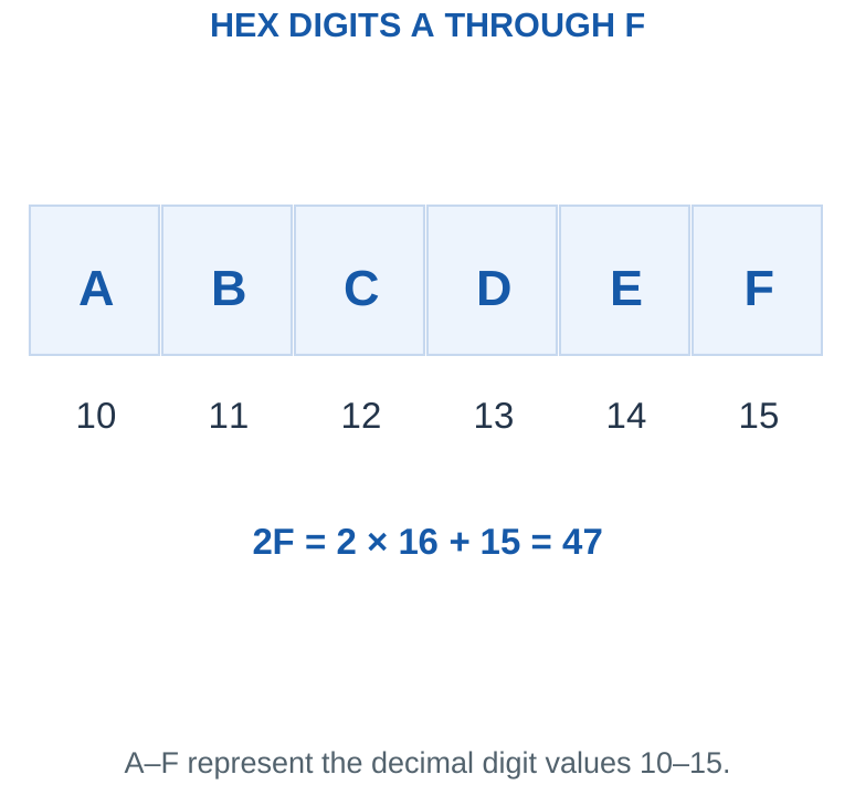
Decimal to hexadecimal: Repeated division by sixteen gives remainders from 0 to 15. Replace remainders 10–15 by A–F, then read the remainders upward. For a fixed width, add leading zeros. A prefix such as 0x is a notation convention, not an extra numerical digit; 0x2F and hexadecimal 2F have the same value.
Hexadecimal to decimal: Multiply each digit value by its appropriate power of sixteen and add. The letter F contributes fifteen times its place value, not six and not a variable. Check that a two-digit hexadecimal unsigned number is between 0 and 255.
Quick check: Two hexadecimal digits cover one byte. FF is decimal 255, while 100 in hexadecimal is decimal 256 and needs nine binary bits.
Worked Problem 4.3: Decimal to Hexadecimal
Problem: Convert decimal 94 to hexadecimal.
Model / approach: Use repeated division by sixteen and letters for remainder values 10–15.
Step 1:
- 94 ÷ 16 = 5, remainder 14 (E)
- 5 ÷ 16 = 0, remainder 5 (5)
Step 2: Read remainders upward: 5E.
Answer: (94)₁₀ = (5E)₁₆.
Check and interpretation: The displayed letters represent digit values. The division quotient and remainder satisfy N = 16q + r at each step, so reversing the remainder order reconstructs the original positional value.
Worked Problem 4.4: Hexadecimal to Decimal
Problem: Convert hexadecimal 3B to decimal.
Model / approach: Replace letters by values and use powers of sixteen.
Step 1: From right to left the contributions are 11 × 1 + 3 × 16.
Step 2: The total is 59.
Answer: (3B)₁₆ = (59)₁₀.
Check and interpretation: A hexadecimal letter is a digit, not a Boolean variable in this question. Keep its digit value separate from its position weight.
6. Binary and Hexadecimal Grouping
Because 16 = 2^4, binary and hexadecimal convert directly through four-bit groups. For an integer binary word, make groups from the right. Add leading zeros to complete the leftmost group if necessary. Convert each group independently and preserve internal zero groups.
Worked check: Check the grouping side
Binary 10101 groups from the right as 0001 0101, giving hexadecimal 15. Grouping from the left as 1010 1000 would introduce trailing zeros and give A8, a different value. Left padding completes a group without moving the original LSB.
| Hex | Binary | Hex | Binary |
|---|---|---|---|
| 0 | 0000 | 8 | 1000 |
| 1 | 0001 | 9 | 1001 |
| 2 | 0010 | A | 1010 |
| 3 | 0011 | B | 1011 |
| 4 | 0100 | C | 1100 |
| 5 | 0101 | D | 1101 |
| 6 | 0110 | E | 1110 |
| 7 | 0111 | F | 1111 |
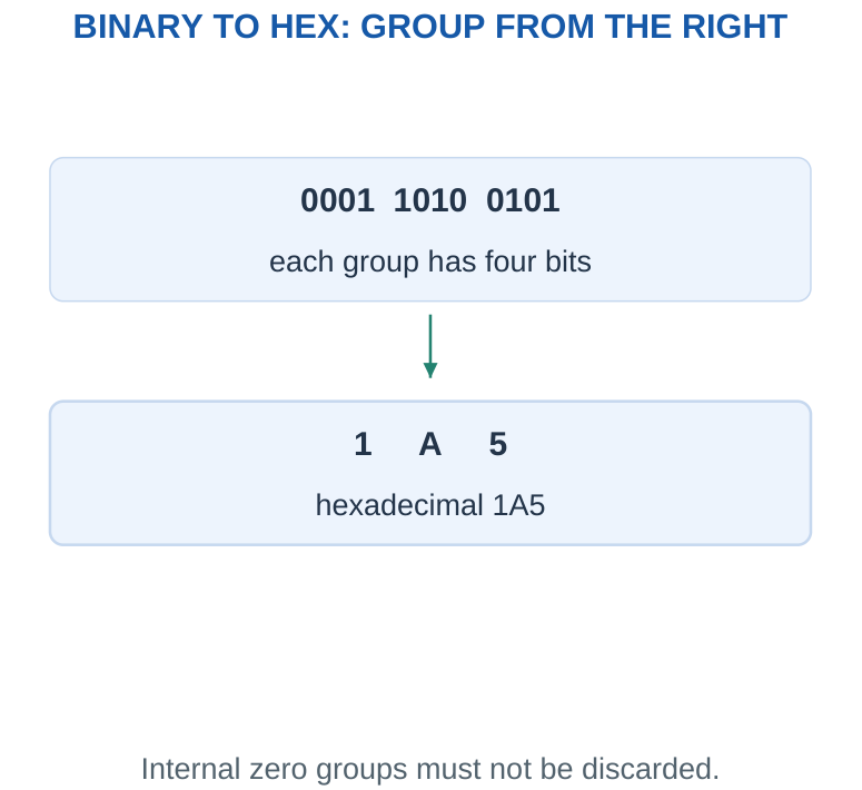
To convert hexadecimal to binary, expand every digit into four bits. Remove only unnecessary leading zeros if no width is specified. Never delete zeros inside the word. A hexadecimal word is compact notation for the same value, not a separate form of arithmetic or a different hardware voltage.
Exam trick: Convert binary to hex by grouping rather than going through decimal. Then use decimal as an independent check when the question is small enough.
Worked Problem 4.5: Binary to Hex by Nibbles
Problem: Convert binary 10110110 directly to hexadecimal.
Model / approach: Group integer bits from the right, padding only on the left.
Step 1: Complete groups: 1011 0110.
Step 2: Nibble values in order: B 6.
Answer: (10110110)₂ = (B6)₁₆.
Check and interpretation: The inserted leading zeros do not change the value. Internal zero nibbles must be preserved, since omitting one would shift a hex digit by a factor of sixteen.
Worked Problem 4.6: Hex to a Fixed-Width Binary Word
Problem: Expand hexadecimal 5A into exactly 8 binary bits.
Model / approach: Every hex digit becomes one four-bit group.
Step 1: Expand each digit: 0101 1010.
Step 2: The combined word is 01011010; its decimal value is 90.
Answer: (5A)₁₆ = (01011010)₂.
Check and interpretation: Preserve all four bits for each digit because the question specifies the width. A leading or internal zero in a group is part of the representation even though it adds no weight by itself.
7. Word Width, States and Representation Range
With n bits there are 2^n different patterns. Under unsigned interpretation, these represent values 0 to 2^n – 1. The minimum width for a nonnegative value N is the smallest n for which N ≤ 2^n – 1, taking at least one written bit for zero.
Worked check: Minimum bits for alternatives
A controller must select among six independent choices. Two bits give only four patterns, while three give eight, so at least three select bits are needed. Two of the eight codes may be unused, but their required behaviour must be specified before treating them as don’t-cares.
Worked check: Bit count and largest value
Seven bits give 128 possible words and unsigned maximum 127. The number 128 itself requires eight bits, written 10000000. A count of states includes zero; confusing the count with the maximum creates an off-by-one error at every power-of-two boundary.
A circuit that selects among M alternatives needs enough selection bits that 2^n ≥ M. Some patterns may be unused when M is not a power of two. Unused does not automatically mean electrically safe, impossible or an allowed don’t-care condition; those conclusions need the specification.
For fixed-width unsigned addition, preserve a carry-out separately. If a four-bit sum needs five bits, the low four bits alone are not the complete mathematical result. A carry-out and signed overflow are different concepts; this unit’s basic addition examples use unsigned values.
Boundary check: Values just below a power of two fit in the previous width. The power itself needs an extra bit: 255 fits in eight bits, but 256 needs nine.
Worked Problem 4.7: States and Maximum Unsigned Value
Problem: Find the number of patterns and maximum unsigned value for 5 bits. How many bits are needed for the next value after that maximum?
Model / approach: Count patterns including the all-zero word.
Step 1: Patterns = 2^5 = 32. Maximum value = 32 – 1 = 31.
Step 2: The next value 32 is binary 1 followed by 5 zeros, requiring 6 bits.
Answer: 32 patterns; range 0–31; next value needs 6 bits.
Check and interpretation: The number of states is one greater than the maximum unsigned value because zero is one of the states. This count does not imply a signed numerical interpretation.
8. Logic Levels and Noise Margins
A logic input recognises ranges rather than one exact voltage. A voltage at or below VIL,max is guaranteed LOW and a voltage at or above VIH,min is guaranteed HIGH within the valid operating and input-voltage conditions. Between these thresholds, the logic state is not guaranteed.
NUMBER REPRESENTATION CHECK
Width: Keep the requested leading zero bits.
Base: Label binary, decimal or hexadecimal.
Direction: Read division remainders upward.
Cross-check: Convert the result back.
For an unsigned N-bit word, the greatest value is 2^N – 1. The all-zero word is included in the state count.
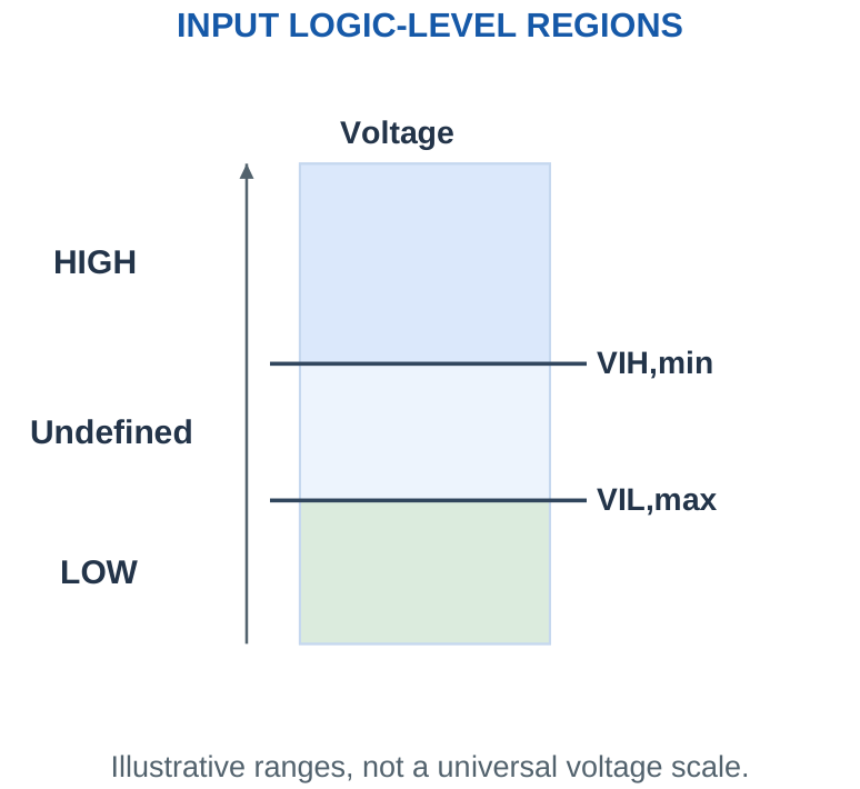
The driver guarantees VOL,max and VOH,min under stated loading. Voltage compatibility requires VOH,min ≥ VIH,min and VOL,max ≤ VIL,max, together with compatible input limits, supplies and current conditions. High-state noise margin is NMH = VOH,min – VIH,min; low-state margin is NML = VIL,max – VOL,max.
Different logic families and supplies have different thresholds. Do not assume that every HIGH is 5 V or that a 3.3 V output can safely drive every 5 V input. A negative margin identifies a failed guarantee. Floating inputs are not reliable 0s and should be given a defined condition appropriate to the circuit.
Numerical convention: Threshold values in the problems are explicitly supplied educational interface specifications. They are not universal values for every microcontroller or CMOS family.
Worked Problem 4.8: Check HIGH and LOW Noise Margins
Problem: Driver VOH,min = 3 V and VOL,max = 0.2 V. Receiver VIH,min = 2.3 V and VIL,max = 0.9 V. Calculate margins and assess the voltage-level guarantee.
Model / approach: Use the guaranteed output/input limits; assume other voltage and current conditions are compatible.
Step 1: NMH = 3 – 2.3 = 0.7 V.
Step 2: NML = 0.9 – 0.2 = 0.7 V.
Answer: Both margins are nonnegative.
Check and interpretation: A nonnegative pair is a voltage-level screen under the supplied conditions, not a complete interface approval. Input-voltage limits, output loading, ground reference and supply sequencing can impose additional conditions.
Worked Problem 4.9: Classify Input Voltages
Problem: Given VIL,max = 0.8 V and VIH,min = 2.0 V, classify inputs 0.3 V, 1.2 V and 2.7 V. All are within absolute input limits.
Model / approach: Use the guaranteed recognition ranges.
Step 1: 0.3 V ≤ 0.8 V: LOW.
Step 2: 0.8 V < 1.2 V < 2.0 V: not guaranteed.
Step 3: 2.7 V ≥ 2.0 V: HIGH.
Answer: LOW, undefined, HIGH in the given order.
Check and interpretation: Undefined does not mean an accepted third logic state. The actual switching threshold and response inside the gap are not established by these two guaranteed limits.
9. Basic Logic Gates and Truth Tables
A logic gate implements a Boolean relationship. AND is 1 only when all its inputs are 1. OR is 1 when at least one input is 1. NOT reverses its single input. NAND and NOR are the complements of AND and OR respectively. XOR is 1 for two unequal inputs.
Worked check: Count truth-table rows
For three independent inputs A,B,C, a complete truth table needs eight rows. For four inputs it needs sixteen. A table with four rows cannot fully specify an unrestricted three-input function unless it uses an explicitly explained shorthand for the omitted combinations.
Worked check: Evaluate complements in order
For Y = (AB)’ and A = B = 1, first calculate AB = 1 and then complement it to get Y = 0. For A = 1, B = 0, AB = 0 and Y = 1. Complementing only B would produce a different function, AB’.
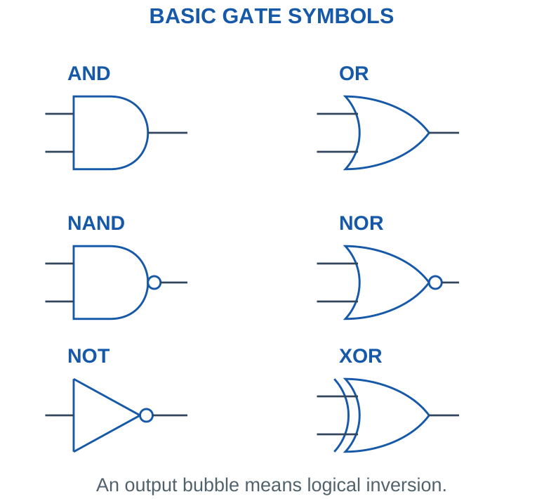
| A | B | AND | OR | NAND | NOR | XOR |
|---|---|---|---|---|---|---|
| 0 | 0 | 0 | 0 | 1 | 1 | 0 |
| 0 | 1 | 0 | 1 | 1 | 0 | 1 |
| 1 | 0 | 0 | 1 | 1 | 0 | 1 |
| 1 | 1 | 1 | 1 | 0 | 0 | 0 |
| A | NOT A |
|---|---|
| 0 | 1 |
| 1 | 0 |
For n independent binary inputs, a complete truth table has 2^n rows. List input patterns in a consistent binary order to avoid missing combinations. Evaluate intermediate gates before the final output when a network has several stages.
Boolean versus arithmetic: An OR gate gives 1 for inputs 1 and 1. A binary adder must produce sum 0 and carry 1 for that same arithmetic input pair; OR alone is not an adder.
Worked Problem 4.10: Evaluate a Gate Network
Problem: For Y = AB + C with A = 1, B = 0, C = 1, find the intermediate AND output and final OR output.
Model / approach: Evaluate the product before the sum.
Step 1: P = A AND B = 1 AND 0 = 0.
Step 2: Y = P OR C = 0 OR 1 = 1.
Answer: P = 0; Y = 1.
Check and interpretation: The + symbol here means OR, not arithmetic addition with carry. Evaluation of one input row is a result for that row; verification of the whole function needs all eight rows.
10. NAND and NOR as Universal Gates
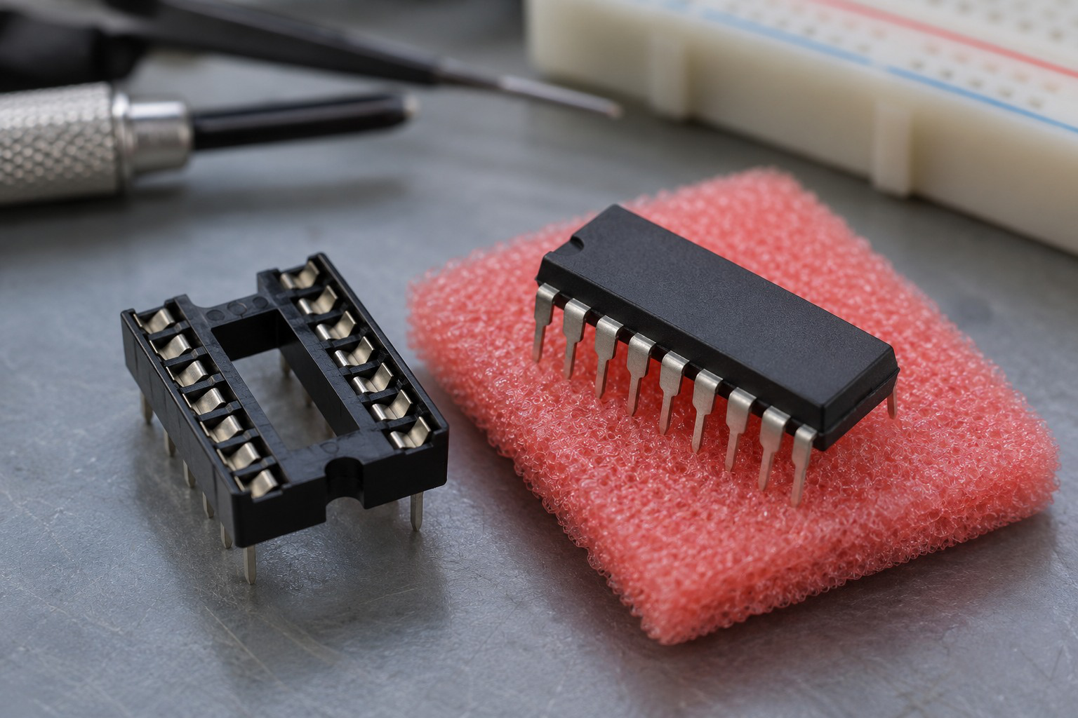
A universal gate type can be connected to realise NOT, AND and OR and therefore any Boolean function. NAND and NOR are both universal. This concerns logical capability, not a claim that every implementation has minimum delay or power.
Worked check: NOT needs one input
The complement of A is A’. It does not depend on B. If a two-variable truth table lists NOT A, the entries repeat across both B values for each fixed A. An extra table column is not a second physical input to the inverter.
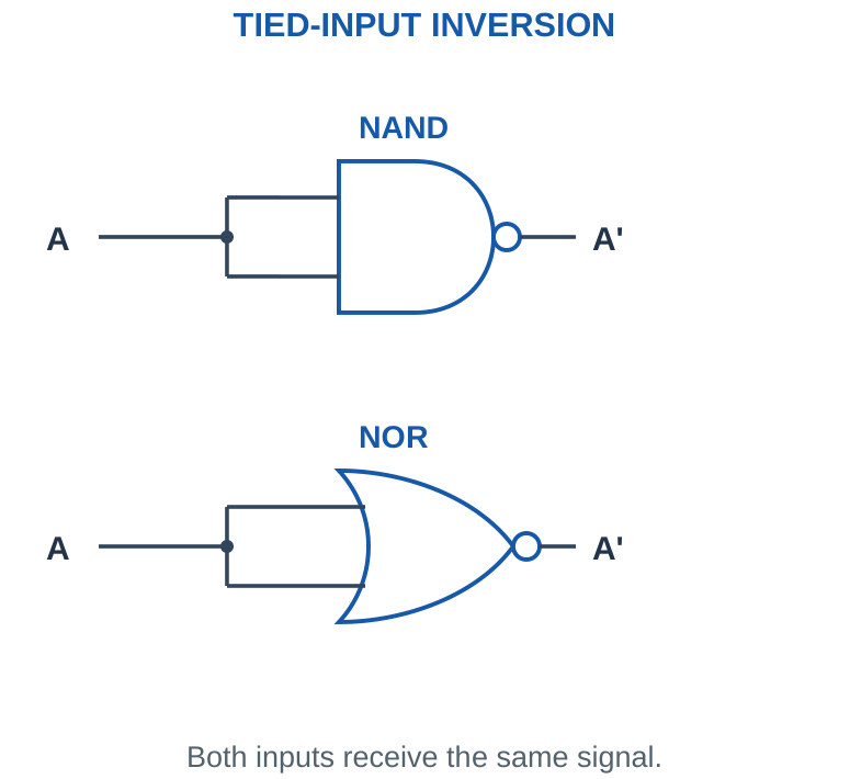
Using NAND: A NAND A = A’; invert a NAND output to obtain AND; and use De Morgan to form OR as NAND(A’, B’).
Using NOR: A NOR A = A’; invert a NOR output to obtain OR; and form AND as NOR(A’, B’).
Tied inputs represent the same signal reaching two pins; do not tie two independent push-pull outputs together. For a sum of products such as AB + CD, a two-level NAND-NAND arrangement naturally uses the complemented product signals (AB)’ and (CD)’ at its final gate. For a product of sums, a NOR-NOR arrangement has a similar role.
Count carefully: A diagram using only NAND gates may still require additional gates to create complemented inputs. State whether those complements are already available when comparing gate counts.
Worked Problem 4.11: Realise NOT Using NAND Only
Problem: Give a NAND-only implementation of NOT and count two-input NAND gates. Assume neither complemented input is already available.
Model / approach: Apply tied-input inversion and De Morgan as needed.
Step 1: Implementation: A NAND A.
Step 2: Required gate count = 1. A repeated complemented product in the AND expression is one shared signal.
Answer: 1 NAND gate(s) realise the stated function.
Check and interpretation: A fan-out branch copies a gate output to multiple inputs; it does not require a duplicate gate unless electrical loading calls for buffering. The truth table of each implementation has been checked for all input combinations.
Worked Problem 4.12: Realise OR Using NAND Only
Problem: Give a NAND-only implementation of OR and count two-input NAND gates. Assume neither complemented input is already available.
Model / approach: Apply tied-input inversion and De Morgan as needed.
Step 1: Implementation: (A NAND A) NAND (B NAND B).
Step 2: Required gate count = 3. A repeated complemented product in the AND expression is one shared signal.
Answer: 3 NAND gate(s) realise the stated function.
Check and interpretation: A fan-out branch copies a gate output to multiple inputs; it does not require a duplicate gate unless electrical loading calls for buffering. The truth table of each implementation has been checked for all input combinations.
11. XOR, Inequality and Parity
For two inputs, XOR is 1 when exactly one input is 1. Its expression is A ⊕ B = A’B + AB’. The output is zero for equal inputs. It is useful for the sum bit in addition and for detecting a single-bit difference.
For more than two inputs, cascaded XOR is an odd-parity function: the output is 1 when an odd number of inputs are 1. “Exactly one” is no longer the general multi-input rule. XOR is associative and commutative. Useful identities are A ⊕ 0 = A, A ⊕ 1 = A’, A ⊕ A = 0 and A ⊕ A’ = 1.
An even-parity bit can be chosen as the XOR of the data bits so that the XOR of data plus parity is zero. This extension illustrates the gate; parity detects an odd number of bit flips but cannot locate an error or detect every even number of flips.
Adder clue: XOR gives the one-bit sum without carry. AND or majority logic produces the carry separately.
Worked Problem 4.13: Generate an Even-Parity Bit
Problem: Data bits are 1011. Find the parity bit P that makes the total number of 1s even.
Model / approach: P is the XOR of all data bits.
Step 1: The data contain 3 ones. Their cascaded XOR is 1.
Step 2: Choose P = 1; total ones including P = 4, which is even.
Answer: P = 1.
Check and interpretation: This is an even-parity convention. An odd-parity convention chooses the opposite bit. Parity checks can detect odd numbers of bit flips but cannot identify which bit changed.
12. Boolean Algebra: Basic Laws
Boolean algebra manipulates logic functions whose variables take 0 or 1. A sum means OR and a product means AND. The laws below simplify circuits without changing their truth table.
| Law | OR Form | AND Form |
|---|---|---|
| Identity | A + 0 = A | A·1 = A |
| Dominance | A + 1 = 1 | A·0 = 0 |
| Idempotent | A + A = A | A·A = A |
| Complement | A + A’ = 1 | A·A’ = 0 |
| Commutative | A + B = B + A | AB = BA |
| Associative | (A + B) + C = A + (B + C) | (AB)C = A(BC) |
| Absorption | A + AB = A | A(A + B) = A |
The two distributive laws are A(B + C) = AB + AC and A + BC = (A + B)(A + C). Double complement gives (A’)’ = A. Boolean expressions need parentheses to show the intended scope of a complement or operation.
Common mistake: A + A is A in Boolean algebra, not 2A. Similarly, A·A is A, not a new numerical square that can take values other than zero or one.
Worked Problem 4.14: Absorption
Problem: Simplify F = A + AB and identify the main Boolean law.
Model / approach: Use valid algebra and preserve the complete complement scope.
Step 1: Factor A + AB = A(1 + B).
Step 2: 1 + B = 1, so the result is A.
Answer: F = A.
Check and interpretation: The original and reduced expressions agree on all eight A,B,C assignments. Variables absent from a particular expression do not affect it. A static reduction does not claim that different physical gate implementations have identical propagation delays.
13. De Morgan’s Theorems
The complement of a product is the sum of the complements: (AB)’ = A’ + B’. The complement of a sum is the product of the complements: (A + B)’ = A’B’. These theorems apply to more inputs by repeating the same operation change and complementing each term.
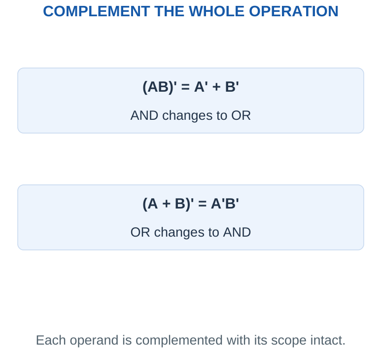
Apply the scope correctly: To complement AB + C, first treat AB as one term: (AB + C)’ = (AB)’C’. Then expand (AB)’ to obtain (A’ + B’)C’. Writing A’B’C’ would wrongly replace the inner product’s complement by another product.
For a nested expression, work from the outermost complement inward and keep parentheses until every scope is clear. Verify the result using a truth table or a few discriminating inputs. A proof requires all combinations or valid algebra; one matching row is only a check.
Memory cue: Break the bar, change the operation, complement each operand. A prime after parentheses complements the entire parenthesised expression, not just the last variable.
Worked Problem 4.15: Complement a Product
Problem: Simplify F = (AB)’ and identify the main Boolean law.
Model / approach: Use valid algebra and preserve the complete complement scope.
Step 1: The outer operation inside the complement is AND.
Step 2: Change it to OR and complement both operands: A’ + B’.
Answer: F = A’ + B’.
Check and interpretation: The original and reduced expressions agree on all eight A,B,C assignments. Variables absent from a particular expression do not affect it. A static reduction does not claim that different physical gate implementations have identical propagation delays.
14. Algebraic Simplification and Circuit Cost
Simplification aims to reduce literals, gates or logic depth while preserving the function. “Simplest” depends on the permitted gate library and the cost measure. A minimal sum-of-products expression is not always the fewest physical packages or the fastest circuit.
Common useful reductions include AB + AB’ = A, A + A’B = A + B, and (A + B)(A + B’) = A. For the second identity, A + A’B = (A + A’)(A + B) = A + B. Show the steps rather than deleting a term without a valid law.
The consensus identity AB + A’C + BC = AB + A’C can remove a logically redundant term. This is a static Boolean statement; physical propagation delays may make a redundant term useful for suppressing a hazard. Deep hazard design is outside this unit, but it explains why minimum logic and best implementation are not always identical.
Good answer format: Write the original expression, the law used, the reduced expression and a clear implementation or verification. Do not confuse Boolean equality with a claim of zero real gate delay.
Worked Problem 4.16: Remove a Covered Branch
Problem: Simplify F = AB + A’B and identify the main Boolean law.
Model / approach: Use valid algebra and preserve the complete complement scope.
Step 1: Factor B(A + A’).
Step 2: The bracket is 1, so the result is B.
Answer: F = B.
Check and interpretation: The original and reduced expressions agree on all eight A,B,C assignments. Variables absent from a particular expression do not affect it. A static reduction does not claim that different physical gate implementations have identical propagation delays.
Worked Problem 4.17: Consensus Term Removal
Problem: Simplify F = AB + A’C + BC and identify the main Boolean law.
Model / approach: Use valid algebra and preserve the complete complement scope.
Step 1: Split BC = ABC + A’BC using A + A’ = 1.
Step 2: AB absorbs ABC, while A’C absorbs A’BC. The BC term is redundant for the static function.
Answer: F = AB + A’C.
Check and interpretation: The original and reduced expressions agree on all eight A,B,C assignments. Variables absent from a particular expression do not affect it. A static reduction does not claim that different physical gate implementations have identical propagation delays.
15. Truth Tables, Minterms, SOP and POS
A minterm is an AND term containing every input variable exactly once, either complemented or uncomplemented. For order A,B,C with A most significant, binary 101 corresponds to minterm m5 = AB’C. A function written Σm(1,3,5) is 1 at precisely those indexed input rows unless don’t-cares are separately stated.
A canonical sum of products (SOP) ORs the minterms for the rows where the function is 1. A canonical product of sums (POS) ANDs maxterms for rows where it is 0. For a zero row 101, its maxterm is (A’ + B + C’), which evaluates to zero at that row. The literal polarity rule is therefore reversed for a maxterm.
A simplified product term need not contain every variable. For instance, A covers all input rows with A = 1. Declare the variable order before converting between decimal indices and literals, especially for a four-variable K-map.
Notation: Σm lists the ON-set; ΠM lists the OFF-set. A function cannot be minimised reliably from a list of indices until the number and order of variables are known.
Worked Problem 4.18: Expand a Canonical SOP
Problem: Variables are A,B, leftmost most significant. Expand F = Σm(1,2) as a canonical SOP.
Model / approach: A 1 bit gives an uncomplemented literal; a 0 bit gives a complemented literal.
Step 1: Binary index words: 01, 10.
Step 2: The corresponding product terms are A’B + AB’.
Answer: F = A’B + AB’.
Check and interpretation: Every canonical product contains every variable exactly once. This is a correct expansion, not necessarily the minimal expression; K-map grouping can remove literals when adjacent minterms combine.
16. Two-Variable Karnaugh Maps
A Karnaugh map places truth-table values so that neighbouring cells differ in one variable. For two variables there are four cells. Use row A = 0,1 and column B = 0,1. Adjacent 1s can be grouped into a product term that omits any variable changing within the group.
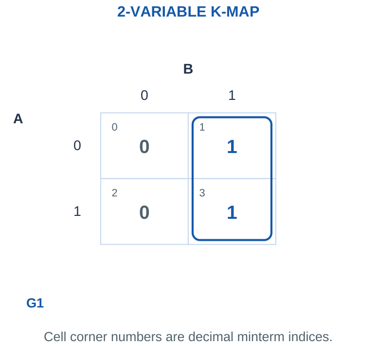
For SOP minimisation, cover every required 1 with rectangular groups of 1, 2 or 4 cells. A group must contain no required zero. A single cell keeps both variables, a pair removes one and the full map gives the constant 1. The all-zero map is constant 0, with no product groups required.
The purpose of a group is to identify constant literals, not merely to draw a box around a convenient set of cells. Read the unchanged row and column values. A variable constant at 1 appears uncomplemented; one constant at 0 appears complemented.
Key habit: After writing the reduced expression, evaluate it over all four rows. A map is a visual method, but the truth table is still the definition of the function.
Worked Problem 4.19: 2-Variable SOP Minimisation
Problem: Minimise F(A,B) = Σm(1,3) as a SOP. Use the stated variable order.
Model / approach: Use Gray order on K-map axes and group ones.
Step 1: Place required ones at [1, 3]; every other cell is zero.
Step 2: Choose valid groups: {1,3}. Each has a power-of-two cell count.
Step 3: Retain the literals constant in each group using the SOP polarity rule. The result is B.
Answer: F = B.
Check and interpretation: The result has been checked on every specified care row. All input rows are specified, so no required zero or one may change.
17. Three-Variable K-Maps and Gray Order
A three-variable map has two rows for A and four columns for BC. Use column order 00, 01, 11, 10. This Gray-code order keeps only one bit different between neighbouring columns, including the first and last columns.
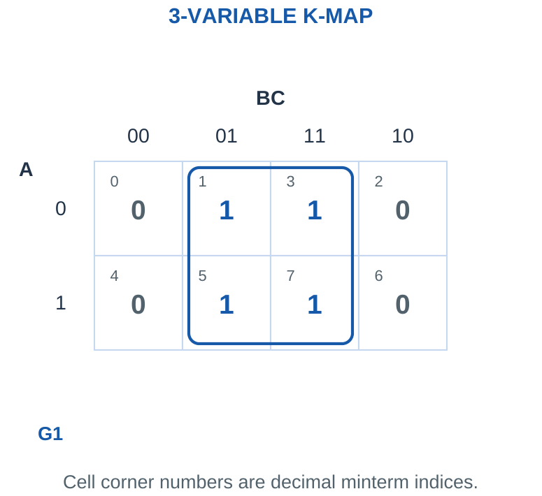
Allowed rectangular groups have 1, 2, 4 or 8 cells. A group of four removes two of the three variables and leaves one literal. Diagonal cells are not adjacent. The left and right edges are adjacent because they differ in one column bit; wraparound grouping follows logic adjacency rather than the printed page boundary.
A group can overlap another group. Every required 1 must be covered, but a 1 may be used more than once when it enables a simpler expression. Keep an isolated 1 as a single minterm if no valid larger group covers it.
Avoid this error: Columns 01 and 10 are not adjacent. Their Hamming distance is two, even though their numerical values may look nearby in a wrongly ordered table.
Worked check: Why the column order matters
For BC columns 00,01,11,10, the first and last columns differ only in B and are adjacent. The middle columns 01 and 11 differ only in B too. The columns 01 and 10 differ in both bits and are not neighbours. Check bit differences rather than decimal closeness.
Worked check: Group size predicts literal count
A group of four in a three-variable K-map leaves one literal. A group of two leaves two literals. This is a useful sanity check: every doubling of a complete valid group removes one changing variable. A proposed four-cell group leaving all three literals has not actually been simplified.
Worked Problem 4.20: 3-Variable SOP Minimisation
Problem: Minimise F(A,B,C) = Σm(1,3,5,7) as a SOP. Use the stated variable order.
Model / approach: Use Gray order on K-map axes and group ones.
Step 1: Place required ones at [1, 3, 5, 7]; every other cell is zero.
Step 2: Choose valid groups: {1,3,5,7}. Each has a power-of-two cell count.
Step 3: Retain the literals constant in each group using the SOP polarity rule. The result is C.
Answer: F = C.
Check and interpretation: The result has been checked on every specified care row. All input rows are specified, so no required zero or one may change.
Worked check: Truth-table check of a reduced term
If a three-variable map reduces to F = C, every odd minterm index must be one because C is the least significant bit. The ON-set is 1,3,5,7. Index 6 is binary 110, so C = 0 and F must be zero there. This checks both variable order and literal polarity.
18. Four-Variable K-Maps
A four-variable map has sixteen cells. Put AB on the rows and CD on the columns, both in Gray order 00, 01, 11, 10. Minterm index is the binary value ABCD, not the row number of the drawing.
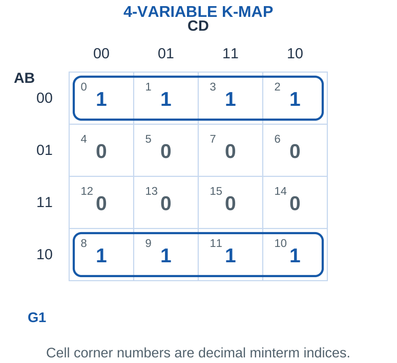
Group sizes and literals: For four variables, groups of 1, 2, 4, 8 and 16 cells leave 4, 3, 2, 1 and 0 literals respectively. Use rectangular powers-of-two dimensions. A group of six cells is invalid in the standard SOP grouping method. No required zero may be included.
Start with large useful groups, cover essential cells and check whether any remaining group adds a new required cell. There may be several equally minimal covers. State one correct minimal expression and justify every retained literal from the group constants.
Coordinate check: The row sequence has minterms 0,1,3,2 in its first row and 4,5,7,6 in its second. The third starts at 12, not 8, because AB = 11.
Worked check: Read an eight-cell group
For four variables, the eight cells whose B bit is zero have minterms 0,1,2,3,8,9,10,11. They reduce to B’. The row bits A,B are not read as decimal row indices: the Gray-ordered bottom row is AB = 10, not 11.
Worked check: Two independent four-cell groups
The cells 0,1,4,5 share A = 0, C = 0 and give A’C’. The cells 10,11,14,15 share A = 1, C = 1 and give AC. Their union is F = A’C’ + AC. B and D disappear because both vary within each group.
Worked Problem 4.21: 4-Variable SOP Minimisation
Problem: Minimise F(A,B,C,D) = Σm(0,1,2,3,8,9,10,11) as a SOP. Use the stated variable order.
Model / approach: Use Gray order on K-map axes and group ones.
Step 1: Place required ones at [0, 1, 2, 3, 8, 9, 10, 11]; every other cell is zero.
Step 2: Choose valid groups: {0,1,2,3,8,9,10,11}. Each has a power-of-two cell count.
Step 3: Retain the literals constant in each group using the SOP polarity rule. The result is B’.
Answer: F = B’.
Check and interpretation: The result has been checked on every specified care row. All input rows are specified, so no required zero or one may change.
Worked check: All sixteen cells
A valid group containing all sixteen cells of a four-variable map gives constant 1. Its zero-literal product is the identity value one. If even one cell is a required zero, the full-map SOP group is forbidden and the result must preserve that zero row.
19. Edge and Corner Grouping
Opposite K-map edges are adjacent. In a four-variable map, the leftmost and rightmost columns can join, as can the top and bottom rows. The four corners form a valid group of four because row adjacency and column adjacency both wrap.
K-MAP GROUP CHECK
Shape: Rectangular power-of-two group.
Adjacency: One-bit change, including wraparound.
SOP: Group required ones; exclude required zeros.
POS: Group zeros with the opposite literal-polarity rule.
A changing variable disappears. A group of 2^k cells removes k variables from that term.
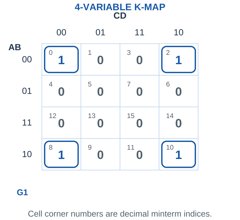
When drawing a wrapped group, use separate visible outlines at the edges and explicitly name the one logical group. It is not four independent single-cell groups. An ordinary diagonal pair in the interior still is not adjacent; edge wrapping does not authorise arbitrary disconnected collections.
To read a group, write all included binary input words and inspect which positions are constant. This gives a reliable algebraic check even when a large wraparound group is hard to visualise. If a proposed group keeps two disconnected values of more than one changing bit without all combinations, it may not be a valid cube.
Corner cue: For rows AB and columns CD in the stated order, the four corners give B’D’. The answer would change if different variables or axis assignments were used.
Worked check: Two wrapped row cells
In a four-variable map, m0 = 0000 and m8 = 1000 differ only in A. Their wrapped vertical pair gives B’C’D’. The map’s top and bottom rows are adjacent, but a pair still removes only one variable; it does not automatically remove both row variables.
Worked Problem 4.22: 4-Variable SOP Minimisation
Problem: Minimise F(A,B,C,D) = Σm(0,2,8,10) as a SOP. Use the stated variable order.
Model / approach: Use Gray order on K-map axes and group ones.
Step 1: Place required ones at [0, 2, 8, 10]; every other cell is zero.
Step 2: Choose valid groups: {0,2,8,10}. Each has a power-of-two cell count.
Step 3: Retain the literals constant in each group using the SOP polarity rule. The result is B’D’.
Answer: F = B’D’.
Check and interpretation: The result has been checked on every specified care row. All input rows are specified, so no required zero or one may change.
Worked check: Two wrapped column cells
Minterms m0 = 0000 and m2 = 0010 differ only in C. Their edge pair gives A’B’D’. The unchanged D bit is zero, so it appears complemented. The pair is valid because the leftmost CD = 00 and rightmost CD = 10 columns are neighbours.
20. Overlap, Essential Groups and Don’t-Cares
An essential prime implicant covers at least one required 1 that no other prime implicant covers. Such a group must be included in a minimal cover. After essentials are selected, cover any remaining 1s economically; overlapping a previously covered cell is allowed.
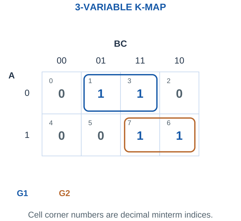
A don’t-care, shown as X, means the specification permits either value for that input combination. It may be used as 1 when it helps make a larger SOP group or ignored when it does not. It need not be covered. Required 1s must still all be covered and required zeros must never enter an SOP group.
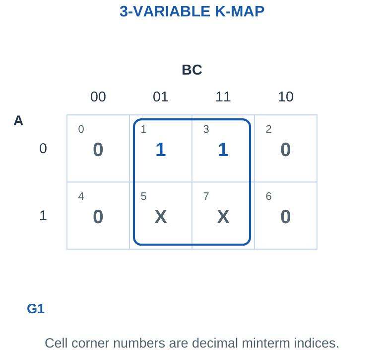
Specification first: An unlisted input is a zero for a fully specified Σm function. It becomes a don’t-care only when the problem explicitly permits it.
Worked Problem 4.23: 3-Variable SOP Minimisation
Problem: Minimise F(A,B,C) = Σm(1,3,6,7) as a SOP. Use the stated variable order.
Model / approach: Use Gray order on K-map axes and group ones.
Step 1: Place required ones at [1, 3, 6, 7]; every other cell is zero.
Step 2: Choose valid groups: {6,7}; {1,3}. Each has a power-of-two cell count.
Step 3: Retain the literals constant in each group using the SOP polarity rule. The result is AB + CA’.
Answer: F = AB + CA’.
Check and interpretation: The result has been checked on every specified care row. All input rows are specified, so no required zero or one may change.
21. POS Minimisation and Zero Grouping
For a product-of-sums result, group zeros instead of ones. The same adjacency, power-of-two size and rectangular grouping rules apply. Each zero group produces a sum term that is zero throughout that group.
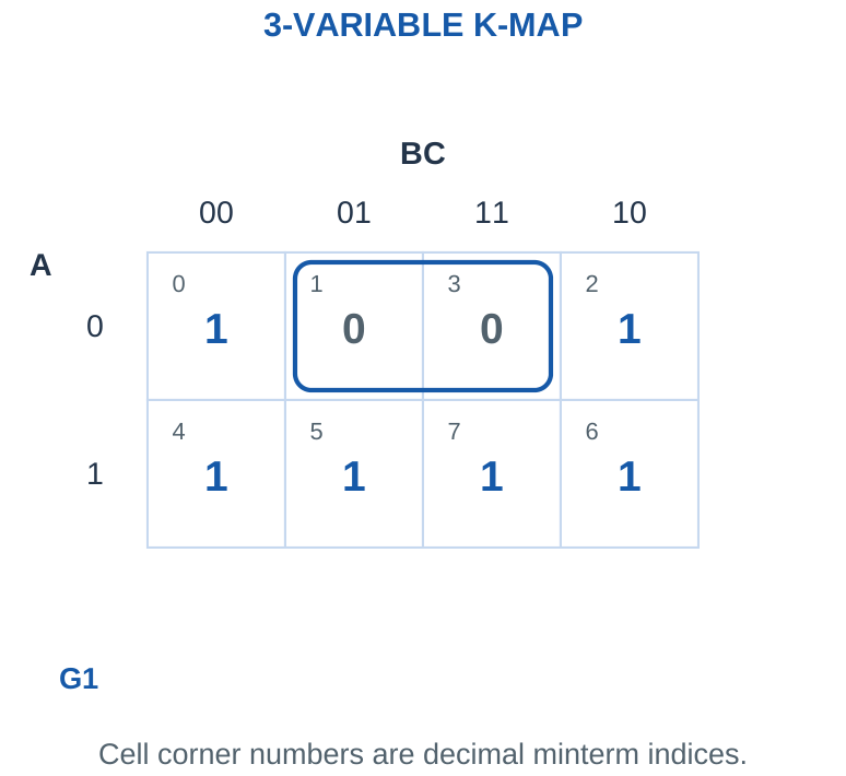
For a zero group, a variable constant at 0 appears uncomplemented in the sum term; a variable constant at 1 appears complemented. This polarity is opposite to SOP one-group reading. AND all the resulting sum terms to obtain the POS expression.
SOP and POS can describe the same truth table with different gate structures. Choose the form requested. Check equivalence over all care rows, especially when don’t-cares allow more than one valid assignment. Do not group 1s and then apply the zero-group literal rule.
One-cell check: For zero row ABC = 101, the sum term is A’ + B + C’. Substituting 1,0,1 makes all three literals zero, confirming the polarity.
Worked check: POS literal polarity
Zero cells m1 = 001 and m3 = 011 share A = 0, C = 1. The sum term must be zero on both, so it is A + C’. B changes and disappears. Using A’C would be the SOP one-group reading, not the required POS zero-group result.
Worked check: Check one maxterm
For the zero row ABC = 101, the canonical maxterm is A’ + B + C’. Substitution gives 0 + 0 + 0 = 0. At any other row at least one literal is one, making that sum term one. This explains the reversed polarity rule for maxterms.
Worked Problem 4.24: 3-Variable POS Minimisation
Problem: Minimise F(A,B,C) = Σm(0,2,4,5,6,7) as a POS. Use the stated variable order.
Model / approach: Use Gray order on K-map axes and group zeros.
Step 1: Place required ones at [0, 2, 4, 5, 6, 7]; every other cell is zero.
Step 2: Choose valid groups: {1,3}. Each has a power-of-two cell count.
Step 3: Retain the literals constant in each group using the POS polarity rule. The result is (A + C’).
Answer: F = (A + C’).
Check and interpretation: The result has been checked on every specified care row. All input rows are specified, so no required zero or one may change.
Worked check: SOP and POS can agree
The expression AB has ones only when both inputs are one. Its canonical POS is (A + B)(A + B’)(A’ + B), formed from its three zero rows. Algebra or all four truth-table rows confirms the equivalence. Canonical form is usually longer than a simplified form.
22. Half Adder: Truth Table and Logic
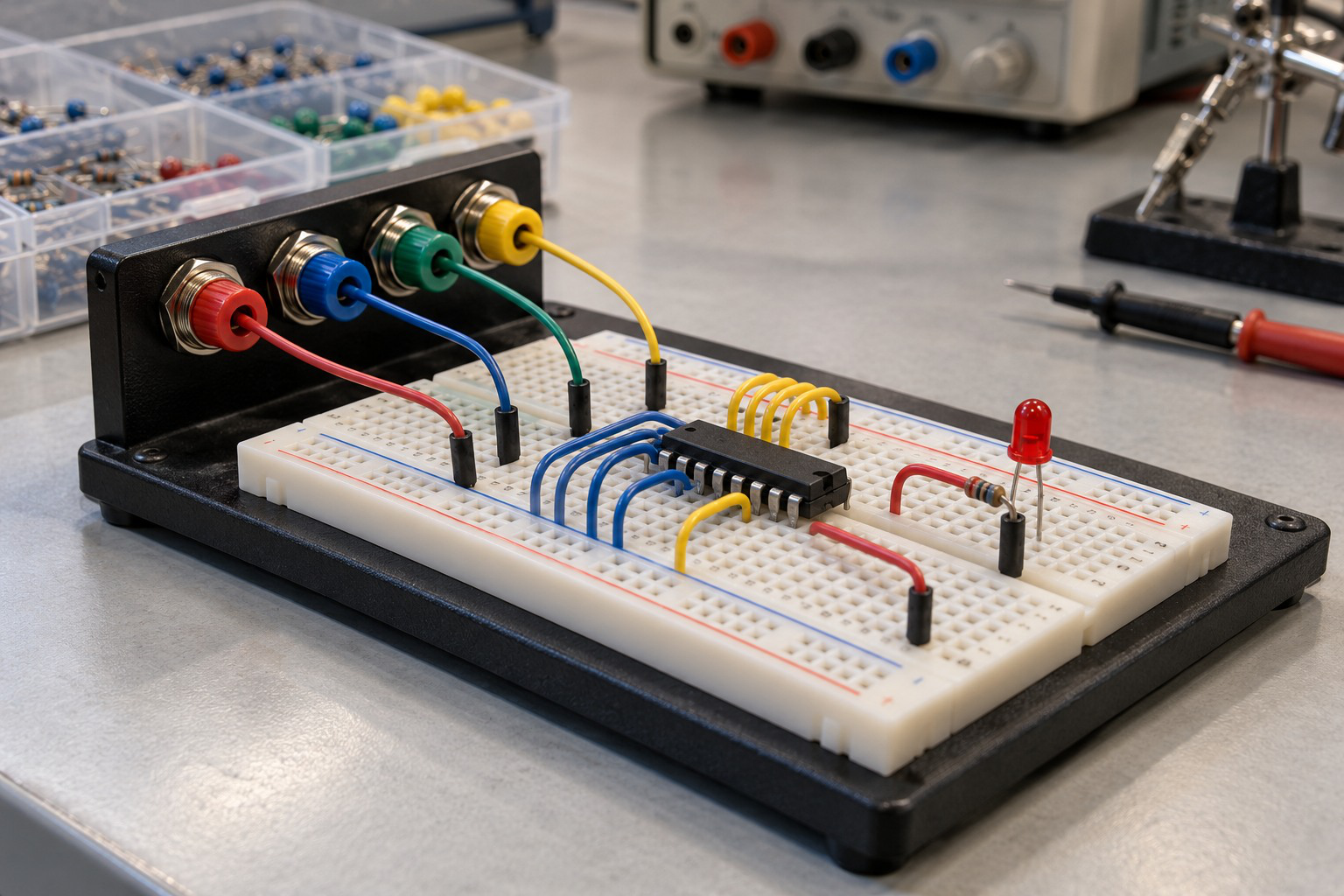
A half adder adds two one-bit numbers A and B. It has two outputs: sum S and carry C. It has no carry input. The complete arithmetic result is the two-bit word CS, not simply S.
Worked check: Half-adder arithmetic value
For A = B = 1, S = 0 and C = 1. The encoded value is 2C + S = 2, not zero. If the carry line is ignored, the reported sum loses information. Always state whether the question wants one sum bit or the complete arithmetic result.
| A | B | S | C |
|---|---|---|---|
| 0 | 0 | 0 | 0 |
| 0 | 1 | 1 | 0 |
| 1 | 0 | 1 | 0 |
| 1 | 1 | 0 | 1 |
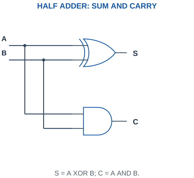
From the table, S = A ⊕ B = A’B + AB’ and C = AB. The identity A + B = S + 2C uses arithmetic addition on the two sides to check the encoded result; it is not the Boolean-OR identity used in a logic expression.
For A = B = 1, the result is binary 10. The sum bit zero is correct because the value two is represented by the carry bit. A half adder alone cannot add an incoming carry from the previous bit of a multi-bit chain.
Answer both outputs: An adder question asking for the result of 1 + 1 is incomplete if the answer reports only sum zero. Include the carry.
Worked Problem 4.25: Half-Adder Output Word
Problem: A half adder receives A = 1, B = 1. Find S, C and the complete binary result.
Model / approach: Use XOR for sum and AND for carry.
Step 1: S = 1 ⊕ 1 = 0; C = 1 AND 1 = 1.
Step 2: Output word CS = 10, with decimal value 2.
Answer: S = 0, C = 1; result 10.
Check and interpretation: The carry has weight two while the sum has weight one. The arithmetic identity A + B = S + 2C confirms that neither bit should be interpreted in isolation.
23. Full Adder: Truth Table and Construction
A full adder adds three one-bit values A, B and Cin. It produces sum S and carry Cout. Cin is the carry from the next lower position; Cout continues toward the next higher position.
| A | B | Cin | S | Cout |
|---|---|---|---|---|
| 0 | 0 | 0 | 0 | 0 |
| 0 | 0 | 1 | 1 | 0 |
| 0 | 1 | 0 | 1 | 0 |
| 0 | 1 | 1 | 0 | 1 |
| 1 | 0 | 0 | 1 | 0 |
| 1 | 0 | 1 | 0 | 1 |
| 1 | 1 | 0 | 0 | 1 |
| 1 | 1 | 1 | 1 | 1 |
Worked check: Majority carry check
A full adder has Cout = 1 when at least two of A,B,Cin are one. For 1,0,1 the carry is one and sum is zero, giving binary 10. For 1,1,1 both carry and sum are one, giving binary 11, decimal three.
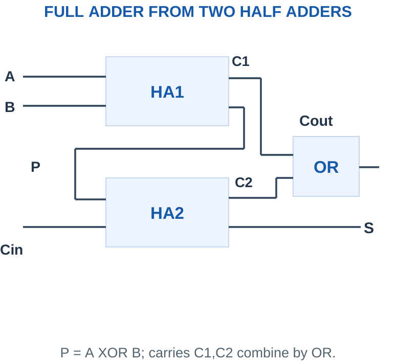
The equations are S = A ⊕ B ⊕ Cin and Cout = AB + Cin(A ⊕ B) = AB + ACin + BCin. Cout is a majority-of-three function: at least two input ones produce carry. The sum is odd parity.
Arithmetic check: For every row, A + B + Cin = S + 2Cout using ordinary integer arithmetic. This independently checks both logic outputs.
Worked Problem 4.26: Full-Adder Intermediate Signals
Problem: A = 1, B = 1, Cin = 1. Find P, S, the two half-adder carries and Cout.
Model / approach: Use the two-half-adder construction.
Step 1: P = A ⊕ B = 0; C1 = AB = 1.
Step 2: S = P ⊕ Cin = 1; C2 = P Cin = 0.
Step 3: Cout = C1 + C2 (OR) = 1.
Answer: S = 1; Cout = 1; output word 11.
Check and interpretation: Check A + B + Cin = S + 2Cout using integer arithmetic. The OR combining carries does not produce an additional arithmetic carry bit.
24. Multi-Bit Binary Addition and Ripple Carry
Build an unsigned n-bit adder by connecting each stage’s carry-out to the next more significant stage’s carry-in. Begin with the LSB and an initial carry, normally zero for ordinary addition. Each position gives one sum bit; retain the final carry separately.
Worked check: Final carry is outside the low word
Four-bit unsigned 1111 plus 0001 produces low result 0000 and carry one. The complete result is 10000, decimal sixteen. Calling the answer simply zero discards the carry. The same fixed-width wrapping idea does not by itself establish signed overflow behaviour.
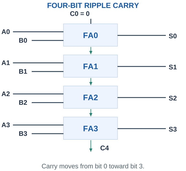
Step-by-step method: At bit i, add Ai, Bi and Ci arithmetically. If the total is 0 or 1, it becomes Si and Ci+1 = 0. If the total is 2 or 3, subtract two for Si and set Ci+1 = 1. Continue until the MSB. Check by converting the complete result, including carry, to decimal.
The name ripple carry describes propagation through successive stages. A simple worst-case educational delay can be estimated from the number of carry stages and their supplied delays. Real timing depends on the particular input paths and gate implementation; do not equate a hand-drawn stage count with a universal device limit.
Width trap: 1111 + 0001 gives 10000. In a four-bit result register the low bits are 0000 with carry 1; the complete unsigned mathematical sum is sixteen.
Worked Problem 4.27: Four-Bit Unsigned Addition
Problem: Add binary 0101 and 0011 with initial carry zero. Give the low four sum bits and final carry.
Model / approach: Begin at bit 0 and propagate each carry toward the MSB.
Step 1: Bit 0: 1 + 1 + carry 0 = 2; S0 = 0, next carry = 1.
Step 2: Bit 1: 0 + 1 + carry 1 = 2; S1 = 0, next carry = 1.
Step 3: Bit 2: 1 + 0 + carry 1 = 2; S2 = 0, next carry = 1.
Step 4: Bit 3: 0 + 0 + carry 1 = 1; S3 = 1, next carry = 0.
Step 5: Decimal check: 5 + 3 = 8.
Answer: Low sum = 1000; carry = 0; complete result = 01000.
Check and interpretation: The leading carry may be zero but is shown separately to expose the fixed-width result. A nonzero carry indicates the complete unsigned sum needs more than four bits.
25. Binary Addition in a CPU ALU
An arithmetic logic unit (ALU) performs selected arithmetic or logical operations on data words. Addition can use a chain of full adders, while AND, OR and XOR operate bit by bit. A selection network chooses the requested result for the output.
STATE IS NOT A PRESENT INPUT
| Block | Question to Ask |
|---|---|
| Combinational | What do the inputs imply now? |
| SR storage | Is it set, reset or holding? |
| D flip-flop | What was D at the active edge? |
Declare the initial state and active levels. Input changes between valid sampling events do not immediately copy through an edge-triggered D element.
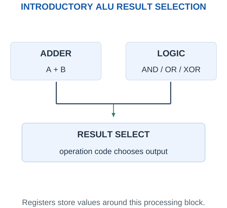
This unit’s ALU model uses unsigned addition and basic logic. For a supplied operation table, decode the select value first, then perform only the corresponding operation. A carry-out belongs to the addition path; it is not inherently a carry output from a bitwise AND or XOR.
For example, AND can clear selected bits, OR can force selected bits to one and XOR can toggle selected bits. These operations depend on the mask and are distinct from numerical addition. A real processor includes status flags and architecture-specific behaviour beyond this introductory model.
Concept check: The ALU is a combinational processing block in this model. Registers around it store operands or results; they are not part of the truth table of an isolated gate.
Worked Problem 4.28: Select a Bitwise ALU Operation
Problem: A four-bit introductory ALU receives A = 1010, B = 1100 and selects AND. Find Y.
Model / approach: Apply the selected operation to corresponding bit positions.
Step 1: From MSB to LSB, compare the pairs in 1010 and 1100.
Step 2: Applying AND gives 1000, unsigned decimal 8.
Answer: Y = 1000.
Check and interpretation: This selected logic result is not the numerical sum of the operands. Any addition carry or processor flag behaviour needs a separate defined operation and architecture.
26. Multiplexer: 2-to-1 Selection
A multiplexer (MUX) routes one of several data inputs to an output under the control of select inputs. For a 2-to-1 MUX, select S = 0 chooses D0 and S = 1 chooses D1. The output equation is Y = S’D0 + SD1.
| Select S | Output Y |
|---|---|
| 0 | D0 |
| 1 | D1 |
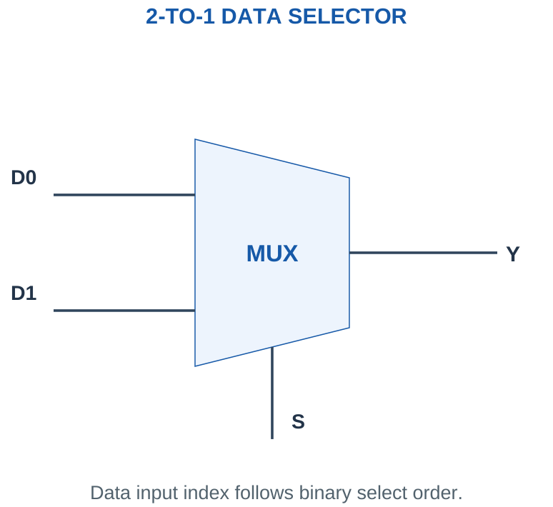
The equation uses two AND terms, one inverter for S and an OR. If the select is known, substitute it before examining the data. If S is unknown and D0 = D1, the logical output is still that common data value; if the data differ, the output cannot be determined without S.
A digital MUX routes logic information. An analog signal multiplexer is a related device category with analog electrical constraints; the Boolean equation alone does not describe every signal-switch specification.
Memory cue: The binary select number names the selected input index. For this conventional positive-logic MUX, S = 0 selects input zero.
Worked Problem 4.29: Evaluate 2-to-1 Selection
Problem: S = 0, D0 = 1, D1 = 0. Find the output of an enabled ideal 2-to-1 MUX.
Model / approach: S = 0 selects D0; S = 1 selects D1.
Step 1: The selected input is D0.
Step 2: Y = S’D0 + SD1 = 1.
Answer: Y = 1.
Check and interpretation: The unselected data value does not affect the settled ideal output for this fixed select. Real transitions may involve propagation delay; the truth table describes the selected logic relationship.
27. Four-to-One MUX and Data Routing
A 4-to-1 MUX has data inputs D0–D3, select bits S1,S0 and output Y. The select word is interpreted as an unsigned index with S1 most significant. An enable input, if present, has behaviour defined by the device; no enable is assumed unless stated.
| S1 | S0 | Y |
|---|---|---|
| 0 | 0 | D0 |
| 0 | 1 | D1 |
| 1 | 0 | D2 |
| 1 | 1 | D3 |
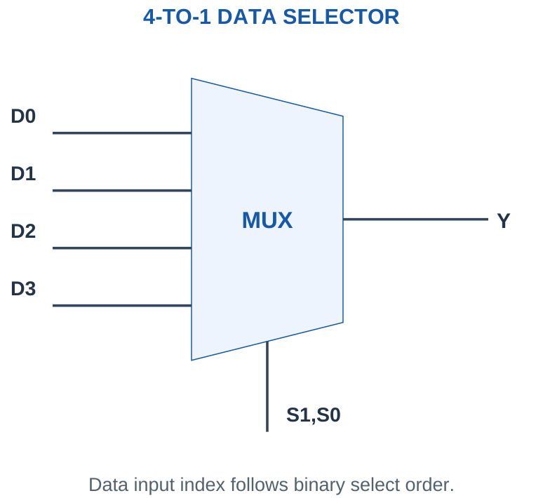
The full equation is Y = S1’S0’D0 + S1’S0D1 + S1S0’D2 + S1S0D3. An 8-to-1 MUX requires three select bits because 2^3 = 8. A wider data bus can use one MUX per bit with shared selection; a 4-bit 2-to-1 bus MUX selects one entire four-bit word.
Distinguish counts: Data input count, select input count and data word width are different quantities. “4-to-1” describes the number of alternative data inputs, not necessarily a four-bit-wide output.
Worked Problem 4.30: Decode a Two-Bit Select
Problem: S1S0 = 10. Data D0,D1,D2,D3 = [0, 1, 1, 0]. Find output of the enabled 4-to-1 MUX.
Model / approach: Treat S1 as the MSB of the data index.
Step 1: Index = 2S1 + S0 = 2.
Step 2: Therefore Y = D2 = 1.
Answer: Y = 1.
Check and interpretation: The data list is in ordinary index order 0,1,2,3. Gray ordering is used for K-map adjacency, not for renumbering the MUX data pins.
28. Realising Boolean Functions with a MUX
A MUX can implement a logic function by connecting data inputs to constants or to remaining variables. For a two-variable function using a 4-to-1 MUX, use the variables as select bits and connect each Di to the function’s truth-table value at that index.
For a three-variable function implemented by a 4-to-1 MUX, choose two variables as selects. For each select combination, inspect the output at remaining variable C = 0 and C = 1. The pair 00 means data constant 0, 11 means 1, 01 means C and 10 means C’. This method avoids guessing connections.
A cascade of smaller MUXes can route more alternatives. For an 8-to-1 selection built from 2-to-1 MUXes, a balanced tree has seven MUX blocks and three selection levels. Logical structure does not remove real propagation delay.
Build from the table: List selected rows in ordinary binary select order, not K-map Gray order, when assigning D0,D1,D2,D3.
Worked Problem 4.31: Three-Variable Function on a 4-to-1 MUX
Problem: Implement F(A,B,C) = Σm(1,2,6,7) using A,B as S1,S0. Find D0–D3 in terms of C.
Model / approach: Inspect the paired outputs for C = 0 and C = 1 at each AB selection.
Step 1: For AB = 00,01,10,11, the C-dependent data are C, C’, 0, 1.
Step 2: Connect D0 = C, D1 = C’, D2 = 0, D3 = 1. Supply C’ with an inverter if needed and not already available.
Answer: (D0,D1,D2,D3) = (C, C’, 0, 1).
Check and interpretation: Each data connection has been checked against both rows of its selected AB pair, verifying all eight input combinations. A constant 1 or 0 must be a valid logic level in the physical implementation.
29. Combinational Logic, State and Memory
A combinational circuit’s settled outputs depend on present inputs. A sequential circuit also depends on stored state. An adder or MUX is combinational; a latch or flip-flop stores a bit. State makes it possible to remember that an event happened after the original input disappears.
A latch is generally level sensitive: its inputs may affect the state while the enabling level is active. An edge-triggered flip-flop updates at the defined clock transition. The terms are sometimes used loosely, so identify the actual circuit and control behaviour rather than relying only on its name.
Q denotes the stored bit and Q’ its complement in valid ordinary states. A state table must identify the present state and the next-state rule. If the initial state is unspecified, a hold command cannot create a known value by itself.
Scope: The syllabus asks for SR and D flip-flop concepts. The following sections explain the basic SR storage core and a clocked D element without transistor-level internal construction.
30. SR Storage Element and Valid States
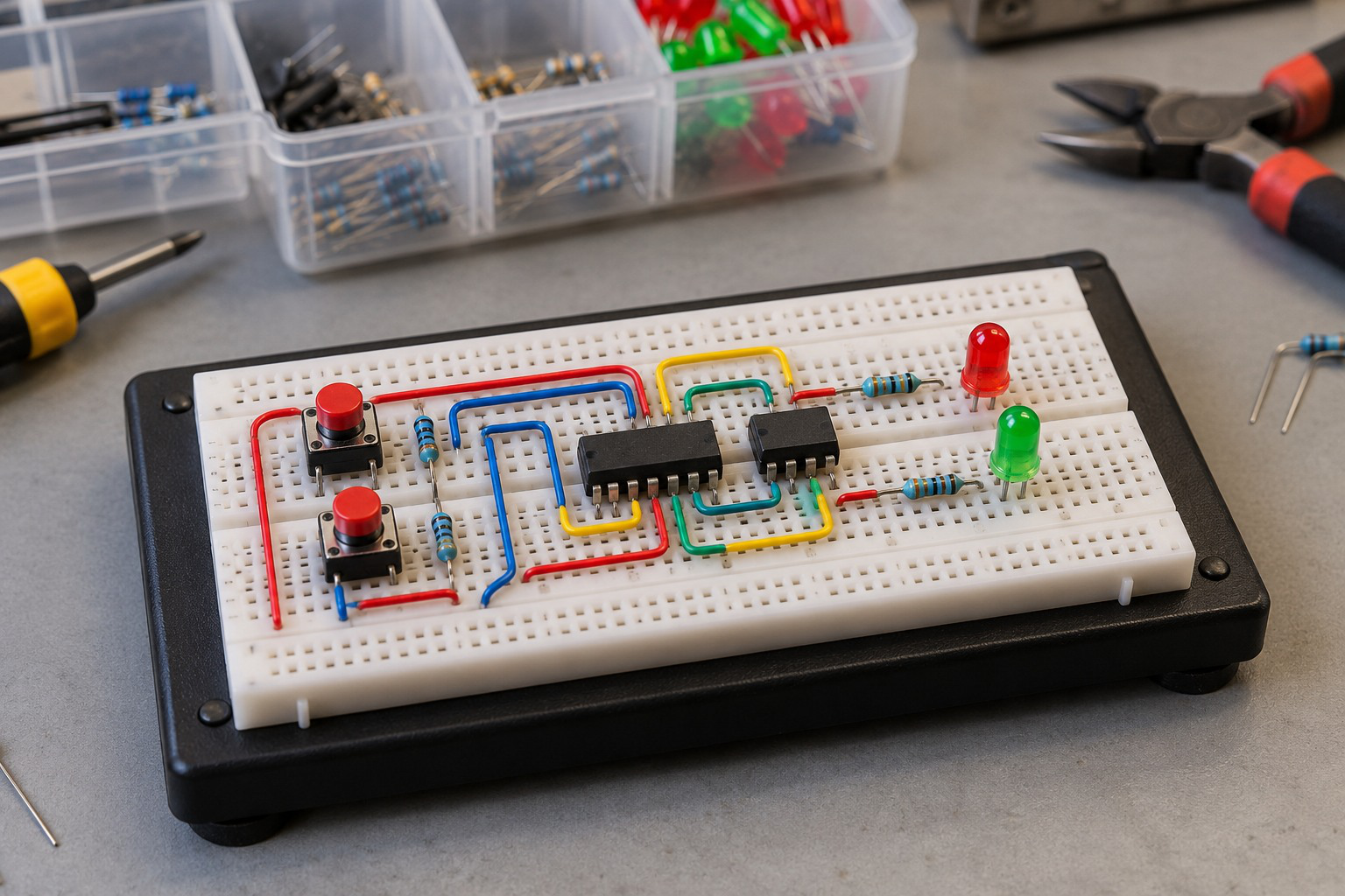
SR means Set and Reset. In an active-HIGH cross-coupled NOR storage core, S = 1, R = 0 sets Q to 1; S = 0, R = 1 resets Q to 0; S = R = 0 holds the previous state. The simultaneous assertion S = R = 1 is forbidden for normal complementary-output operation.
| S | R | Next Q | Meaning |
|---|---|---|---|
| 0 | 0 | Present Q | Hold |
| 0 | 1 | 0 | Reset |
| 1 | 0 | 1 | Set |
| 1 | 1 | Invalid | Both NOR outputs forced LOW |
Worked check: Initial state matters
A NOR SR core given S = R = 0 holds Q. If Q was one it stays one; if it was zero it stays zero. Without an initial state or a preceding valid set/reset event, the hold command leaves Q unknown. Do not replace unknown history with an invented reset.
Worked check: Compare NAND and NOR conventions
An active-HIGH NOR SR core holds at S,R = 0,0. An active-LOW NAND SR core holds at its barred inputs 1,1. Their forbidden simultaneous assertions also differ. A state table is meaningful only with the named gate type and input active levels.
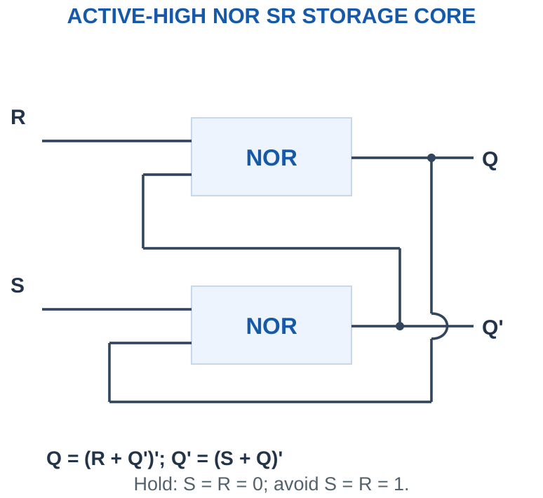
The cross-coupled NOR core is a latch, not inherently an edge-triggered flip-flop. A clocked or gated SR arrangement adds a defined control condition. For an active-LOW NAND SR core, the inactive inputs are 1,1 and both LOW is forbidden; do not reuse the active-HIGH table without changing the input convention.
When both NOR inputs are asserted, Q and Q’ are both zero. When both are released together, the eventual state is not reliably determined by the ideal table. Do not claim the invalid state is a third stable data value or automatically resolves to reset.
State-sequence rule: Carry the previous Q forward through every HOLD row. A hold row is not synonymous with output zero.
Worked Problem 4.32: Trace Active-HIGH SR State
Problem: The NOR SR core begins at Q = 0. Apply S,R pairs [(1, 0), (0, 0), (0, 1), (0, 0)] in order. Find Q after each pair.
Model / approach: Use active-HIGH set/reset and carry state through hold rows.
Step 1: S,R = 1,0: SET gives Q = 1.
Step 2: S,R = 0,0: HOLD gives Q = 1.
Step 3: S,R = 0,1: RESET gives Q = 0.
Step 4: S,R = 0,0: HOLD gives Q = 0.
Answer: Q sequence: 1, 1, 0, 0.
Check and interpretation: No pair asserts S and R simultaneously, so the sequence stays within the valid state table. An active-LOW NAND core would require a different table and different inactive levels.
31. D Flip-Flop: Sampling a Data Bit
A D flip-flop stores the value at D on the specified active clock edge. For the positive-edge-triggered model here, Qnext = D at a rising edge. Between rising edges Q retains its previous value, provided asynchronous controls are inactive.
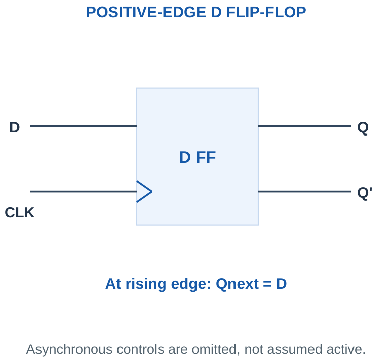
| Event | Next Q |
|---|---|
| Rising clock edge | Sample D |
| No rising edge | Hold present Q |
The D input must meet setup and hold timing around the edge. An input transition too near that edge may violate the specification; the next value cannot then be guaranteed by the simple ideal sampling rule. The output changes after a finite clock-to-Q delay rather than instantaneously.
Some devices add asynchronous preset or clear. These act independently of the normal clocked data rule and have their own active levels and restrictions. No such controls are assumed in a basic D example unless explicitly stated.
Do not confuse: A D latch follows D throughout its active enable level. A D flip-flop samples only at its active edge. The two can give different outputs for the same waveform.
Worked Problem 4.33: Sample a D Sequence
Problem: A positive-edge D flip-flop begins Q = 0. D is stable at the four rising edges with values [1, 0, 1, 1]. No asynchronous control is active. Find Q after each edge.
Model / approach: At each valid rising edge, copy D into stored Q.
Step 1: At rising edges 1 through 4, sampled values are 1, 0, 1, 1.
Step 2: Between those edges, retain the last sampled value; changes at D alone do not immediately alter Q.
Answer: Q after the edges: 1, 0, 1, 1.
Check and interpretation: Setup and hold are assumed satisfied. A falling clock edge is not an update event for this positive-edge model. Q before the first edge is the given initial state.
32. Timing Diagrams and Sampling Checks
A timing diagram shows the order of logic changes. Mark the active clock edges first, read D immediately before each valid sampling edge and carry the resulting Q level forward until the next active event. Ignore falling edges for the positive-edge model unless an asynchronous control is specified.
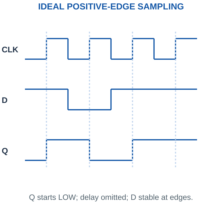
If a rising edge occurs at time te, setup time tsu requires stable data over the interval before te, and hold time th requires stability afterward. A data transition within the required aperture violates the stated timing guarantee. Exactly at a boundary, follow the given inequality and retain practical margin rather than claiming a universal tolerance.
For a simple register-to-register path, a supplied timing model may require Tclk ≥ tCQ,max + tlogic,max + tsu, ignoring clock skew and other specified margins. This is a useful application extension; a hold check is separate and concerns minimum path delay.
Sequence check: An initial Q is needed before the first sampling edge. If it is not specified and no reset is given, write unknown until a valid edge establishes a value.
33. Digital Signals in Microcontroller I/O
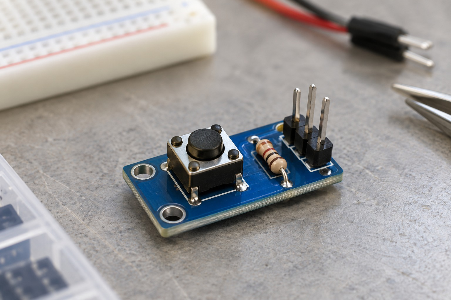
A GPIO pin can act as a digital input or output under controller configuration. An input interprets a voltage using its thresholds. An output attempts to drive a defined level within its current and voltage capabilities. Pin configuration and the external wiring decide which role applies.
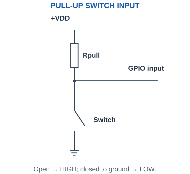
A pull-up resistor connects the input to a positive supply. With an ideal open switch and negligible input current, the input is HIGH. Closing the switch to ground makes it LOW and sends current through the resistor. Pull-down arrangements reverse the default. Mechanical switches may bounce, so one physical action can create several transitions without debouncing.
A binary output cannot automatically supply a motor or relay directly. Logic voltage compatibility, load current and a suitable driver remain necessary. Bit masks can be interpreted conceptually without programming: AND can test selected bits and OR can set selected output bits.
Active-LOW reminder: In the shown pull-up circuit, logical zero means “pressed”. The logical meaning of a status bit must come from the application, not only the physical HIGH/LOW label.
Worked Problem 4.34: Pull-Up Switch Current
Problem: A GPIO input uses a pull-up R = 10000 Ω to 3.3 V and an ideal switch to ground. Neglect input leakage. Find input state open and closed, and closed-switch resistor current and power.
Model / approach: The closed switch places the full supply across the pull-up resistor.
Step 1: Open switch: input ≈ 3.3 V, interpreted HIGH with compatible thresholds. Closed: input ≈ 0 V, LOW.
Step 2: Iclosed = 3.3/10000 ≈ 0.33 mA.
Step 3: PR = VS²/R ≈ 1.089 mW.
Answer: Open HIGH, closed LOW; current ≈ 0.33 mA.
Check and interpretation: This is an active-LOW pressed signal. The resistor limits the grounded-switch current; omitting it would create a direct supply short in this ideal wiring. Contact bounce and actual leakage are separate checks.
34. PLA and PLD Basics
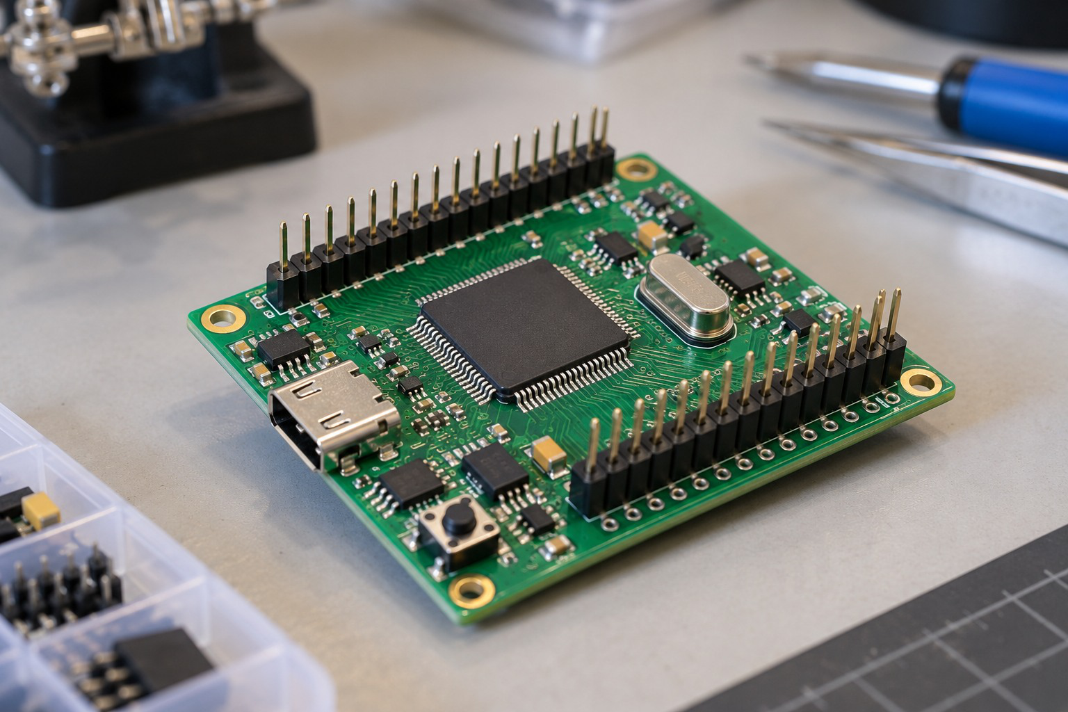
A programmable logic device (PLD) implements logic functions through configurable internal connections. A programmable logic array (PLA) is an introductory two-level example: an AND plane forms selected product terms and an OR plane combines them into outputs. A PLA allows configuration of both planes.
Worked check: Product sharing saves repeated terms
For F1 = AB + A’C and F2 = AB + BC, generate AB once and route it to both output OR functions. The three distinct products are AB, A’C, BC. Counting four occurrences separately misses sharing; counting only two would omit a required product.
Worked check: PLA is a PLD architecture
A PLA configures product generation and product-to-output sums. PLD is the broader category. A classic PAL has a programmable AND plane with fixed OR structure. These introductory distinctions describe architecture, not interchangeable electrical specifications or a universal programming procedure.
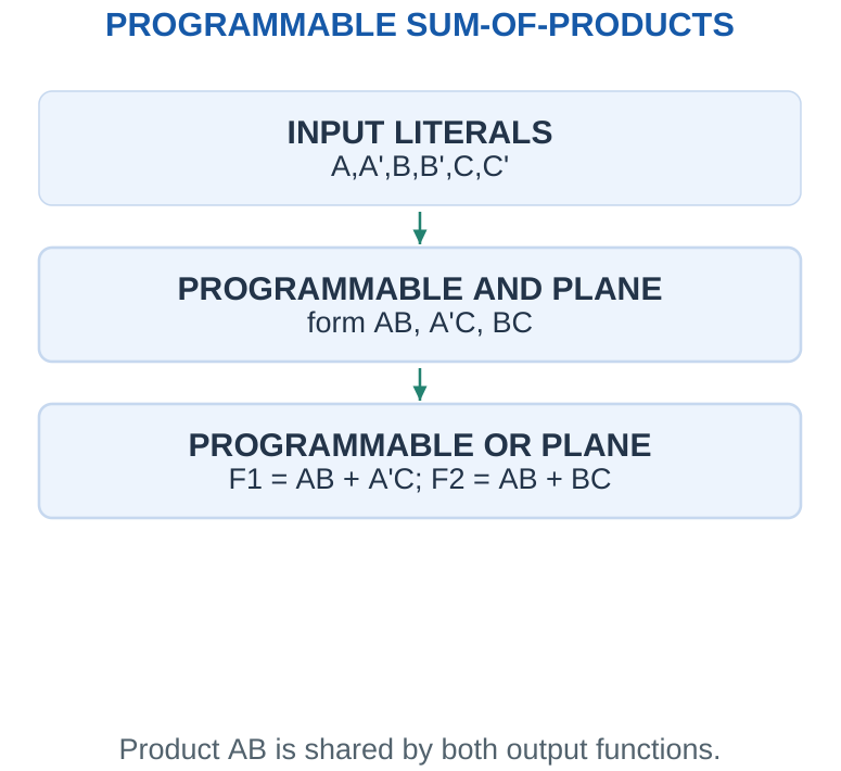
For outputs F1 = AB + A’C and F2 = AB + BC, the shared product AB can be generated once and connected to both output sums. This illustrates multi-output logic organisation. An unused input in a product term is omitted; it is not simultaneously connected as both true and complemented literals in an ordinary useful product.
PLD is a family term rather than a synonym for one PLA architecture. A classic PAL has a programmable AND plane and a fixed OR structure, while other devices have different organisations and may include storage. The basic syllabus requirement is the concept of configurable logic, not a particular programming tool or device pinout.
Distinguish tasks: A MUX selects data under present control inputs. A PLA is configured to implement Boolean relationships. They can both realise logic but organise it differently.
Worked Problem 4.35: Shared Product Terms in a PLA
Problem: Outline a PLA implementation for F1 = AB + A’C and F2 = AB + BC. Count distinct product terms before and after sharing.
Model / approach: Generate each distinct AND product once and connect it to the required OR outputs.
Step 1: The distinct products are AB, A’C, BC.
Step 2: Independent output construction lists four product occurrences; sharing requires only 3 distinct AND terms. Connect each term to the output sums that require it.
Answer: 3 distinct product terms and two output OR functions.
Check and interpretation: The product-term count is a logical organisation measure, not the complete transistor or package count. A real device also has limits on input literals, product terms and output connectivity.
35. [B & C] Analog-to-Digital Conversion: The Signal Bridge
An analog signal varies over a continuous range of values; a digital representation uses discrete symbols. Sampling chooses when a measurement is taken, and quantisation assigns it to one of a finite set of amplitude codes. More bits increase the number of codes; they do not automatically correct sensor error or interference.
An N-bit ADC provides 2^N codes, normally numbered 0 to 2^N – 1. In the explicitly ideal unipolar step model used here, q = Vref/2^N. For 0 ≤ Vin < Vref, code C = floor(Vin/q), clipped to the permitted code range. Real converters have device-specific transfer, offset and gain errors.
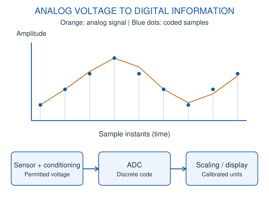
For this model, code C describes the interval Cq ≤ Vin < (C + 1)q. The lower edge is Cq and its midpoint is (C + 0.5)q. By contrast, a separately declared endpoint calibration can use C/(2^N – 1) to map the lowest and highest codes onto physical endpoints. These are different conventions; state which one is used.
Signal chain: Sensor → suitable excitation/conditioning → ADC input → numerical conversion → engineering units → display or control decision. Keep the input inside its allowed range, provide a suitable reference and filter unwanted frequencies before sampling. An analog pin is a measurement interface, not a direct connection for an arbitrary industrial voltage.
Practical example: A classic 10-bit Arduino-style input returns values from 0 to 1023 when configured accordingly. Board reference voltages, resolution and input tolerances vary; do not assume every Arduino uses the same 5 V input range. The converter measures voltage, while calibration establishes temperature, pH or moisture meaning.
Memory cue: 2^N tells how many codes exist; 2^N – 1 is the largest code index. Sampling frequency describes time resolution, while bit depth describes amplitude coding.
Worked Problem 4.36: Eight-Bit ADC Code
Problem: Use an ideal unipolar 8-bit step quantiser, Vref = 3.3 V and Vin = 0.825 V. Find q and code.
Model / approach: q = Vref/256; C = floor(Vin/q).
Step 1: q = 3.3/256 = 0.012890625 V.
Step 2: Vin/q = 64 exactly; floor gives 64.
Answer: q = 12.890625 mV; code 64 = binary 01000000.
Check: The largest permitted code is 255, not 256.
Worked Problem 4.37: Ten-Bit Voltage Step
Problem: An ideal 10-bit converter uses Vref = 5 V. Find number of codes, largest index and nominal step.
Model / approach: Distinguish count from maximum index.
Step 1: 2^10 = 1024 codes; largest code = 1023.
Step 2: q = 5/1024 = 0.0048828125 V.
Answer: 1024 codes; maximum index 1023; step 4.8828125 mV.
Check: This step model does not use 5/1023.
Worked Problem 4.38: Voltage Interval from a Code
Problem: For the preceding ideal step model, find the input interval and midpoint for code 512.
Model / approach: Cq is the lower edge; (C + 1)q is the upper edge.
Step 1: Lower edge = 512 × 5/1024 = 2.5 V.
Step 2: Upper edge = 513 × 5/1024 = 2.5048828125 V.
Step 3: Midpoint = 2.50244140625 V.
Answer: 2.500000 ≤ Vin < 2.5048828125 V; midpoint about 2.502441 V.
Check: One code describes an interval, not an exact unique original voltage.
36. [B & C] Microcontroller: Input, Decision and Output
A microcontroller integrates a processor, program/data memory and peripherals such as GPIO, timers and an ADC in one device. A development board adds supporting power, connectors and communication hardware. A PLC is a controller system designed around industrial I/O and execution requirements; the two terms are not interchangeable.
Inputs: A digital pin recognises a compatible LOW or HIGH signal. An analog input channel converts a permitted voltage into a code. A pushbutton with a pull-up may be active LOW; distinguish electrical level from the meaning of the event. Floating inputs have no guaranteed intended state.
Processing: Acquire the input, apply scaling and the required logical rule, then update the output command. The functional sequence can repeat continuously or on a schedule. Explain the algorithm without requiring a particular programming language.
Outputs: A GPIO supplies a logic command within limited voltage/current ratings. A pump, relay coil, motor or valve usually needs an appropriate driver and its own load-energy path. Digital HIGH does not mean unlimited current. Use protection suitable for the specified load and supply.
A useful functional map labels the measured variable, raw code, calibrated value, threshold, command and physical actuator separately. Power supplies and signal returns must be compatible with the chosen interface; isolation may be needed for a separate domain.
Common error: Treating every analog sensor as a digital switch. The analog reading must first be converted and interpreted. Conversely, a compatible switch signal does not need a fabricated temperature calibration.
37. [B & C] LCD and Seven-Segment Displays
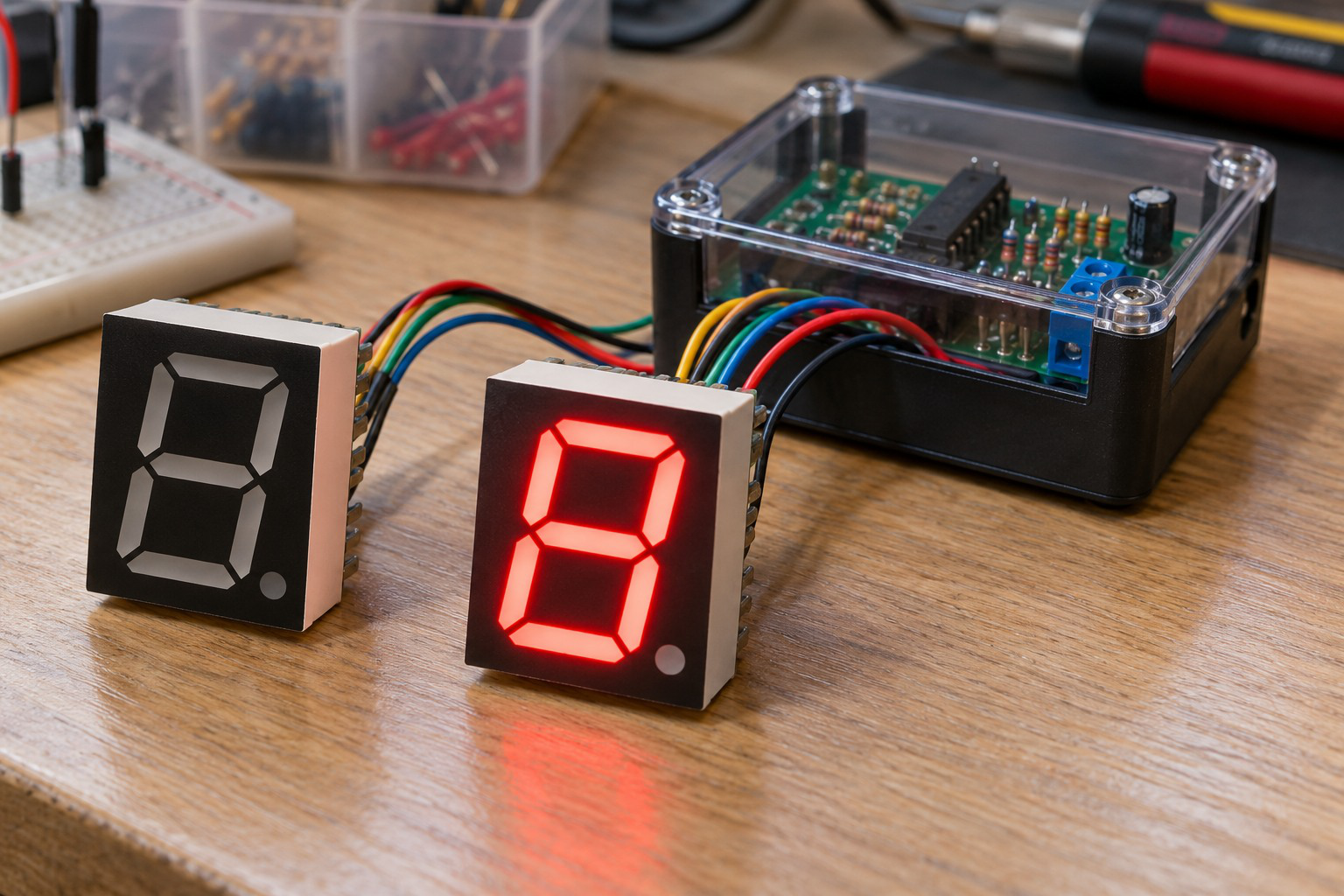
A seven-segment display arranges segments a–g around a digit. The decimal point is normally a separate element. A decoder/driver translates a digit code into the required segment pattern. Common-anode and common-cathode versions use different drive polarity.
For the segment labels shown in the illustration:
- 0: Lights a,b,c,d,e,f.
- 1: Lights b,c.
- 2: Lights a,b,d,e,g.
- 3: Lights a,b,c,d,g.
- 4: Lights b,c,f,g.
- 5: Lights a,c,d,f,g.
- 6: Lights a,c,d,e,f,g.
- 7: Lights a,b,c.
- 8: Lights all seven.
- 9: Lights a,b,c,d,f,g.
TWO ADC CONVENTIONS
| Model | Use |
|---|---|
| Ideal equal-width steps | q = Vref/2^N; code labels voltage intervals |
| Declared endpoint scaling | Map code 0 and code 2^N – 1 to supplied physical endpoints |
State the convention first. Quantisation resolution, sensor accuracy and display rounding are separate properties.
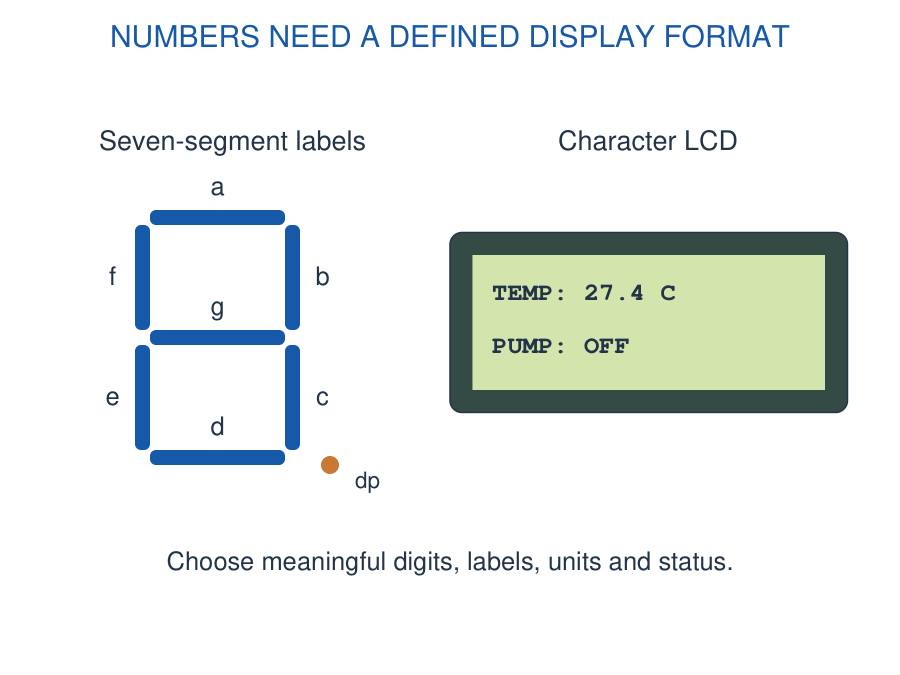
Provide suitable current limiting and driver capability. A multi-digit display may be multiplexed by enabling digits in succession; the perceived steady reading results from sufficiently rapid refresh. A data-routing MUX and a multiplexed display are related selection ideas but different complete circuits.
A character LCD can show labels, numbers, units and status messages. A nominal 16 × 2 display has two rows of sixteen character positions. Numeric conversion, sign, decimal position and unit placement are part of the presentation logic.
Display quality: Show the measurement unit and status, choose useful precision and reserve a clear indication for an invalid or disconnected sensor. More printed decimal places do not create more measurement accuracy. A display reports processed data; it is not itself the sensing element.
Worked Problem 4.39: Seven-Segment Digit
Problem: Using conventional a–g labels, which segments show decimal 3, and how many are lit? Ignore the decimal point.
Model / approach: Select the standard digit pattern.
Step 1: The top, upper-right, lower-right, bottom and centre are a,b,c,d,g.
Step 2: Count these five segments.
Answer: a,b,c,d,g; 5 segments lit.
Check: Common-anode versus common-cathode changes drive polarity, not the visible segment pattern.
Worked Problem 4.40: LCD Character Allocation
Problem: A 16 × 2 LCD must show the 22-character message TEMPERATURE SENSOR OK! including spaces and punctuation. Can it fit on one row? Give one valid split.
Model / approach: Count characters against each row capacity.
Step 1: The complete message needs 22 positions, so it exceeds one row.
Step 2: Use row 1: TEMPERATURE (11 characters). Row 2: SENSOR OK! (10 characters).
Answer: It fits on two rows with the interword separating space represented by the row break.
Check: A newline is a layout instruction; it is not an additional visible cell.
38. [B] Boolean Control and PLC Ladder Concept
Define every input meaning before writing a Boolean rule. Let A = 1 mean a run request and E = 1 mean emergency-stop condition active. The introductory permission rule is M = A E’. If either the request is absent or the stop condition is active, the motor command is zero.
Ladder logic represents Boolean conditions with contacts and output coils between rails. In the abstract interpretation used here, a normally-open instruction is true when its addressed Boolean is 1; a normally-closed instruction is true when that Boolean is 0. Series conditions implement AND; parallel branches implement OR.
CONTROL-CHAIN CHECK
Input: Identify physical meaning and polarity.
Conversion: Turn the signal into a valid code.
Calibration: Express the measurement in units.
Decision: Apply logic, threshold and history.
Output: Use a driver suitable for the load.
A digital output is a command interface. It does not provide arbitrary actuator power.
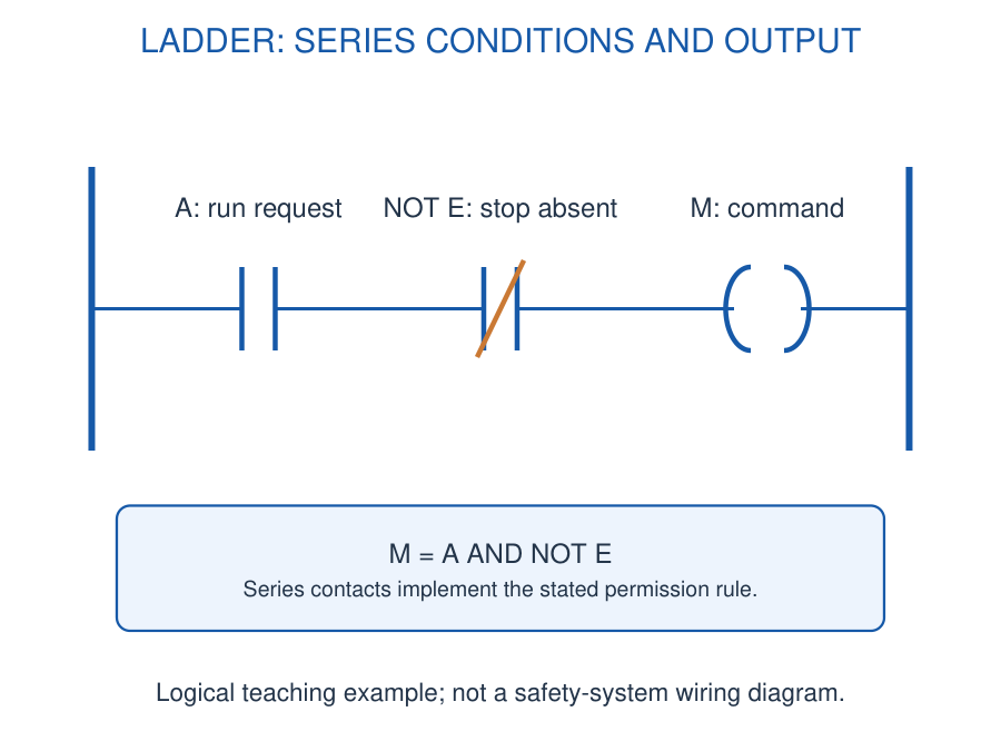
A software contact symbol is not a complete specification of a physical switch. A real emergency-stop system requires an appropriate safety architecture. The simple classroom equation describes a logical command only; it does not establish a safety-rated stop function.
A PLC cyclically acquires relevant inputs, executes its logic and updates outputs, along with communication/diagnostics. The precise scan boundary, I/O refresh order and direct-I/O behaviour depend on the controller. An input snapshot explains why a mid-cycle physical change may wait until a later refresh.
Sequence: Define the machine condition → assign input meanings → write a truth table → express the Boolean function → draw the ladder representation → check every required row. Keep start/stop memory, interlocks and timing distinct from a purely combinational permit.
Automated ON/OFF: A temperature request can command a fan only when an enable is active. A pressure alarm can combine high pressure OR sensor fault. Such expressions must follow the stated meanings and polarity, not just the names printed on inputs.
Worked Problem 4.41: Run-Request Interlock
Problem: Let A = 1 mean run request and E = 1 mean stop condition active. For M = AE’, find M for (A,E) = (1,0), (1,1), (0,0).
Model / approach: Evaluate the complement before the AND.
Step 1: For (1,0), E’ = 1 so M = 1.
Step 2: For (1,1), E’ = 0 so M = 0. For (0,0), A = 0 so M = 0.
Answer: M = 1, 0, 0 respectively.
Check: This is a logical permit, not a complete safety-rated motor-control design.
Worked Problem 4.42: Parallel Requests with Enable
Problem: A and B are alternative requests; H = 1 means enable. Write Y and evaluate A = 0, B = 1, H = 1.
Model / approach: Parallel requests implement OR; the enable is a series AND condition.
Step 1: Y = (A + B)H.
Step 2: A + B = 1; multiplying by H = 1 gives 1.
Answer: Y = (A + B)H; tested output HIGH.
Check: If H becomes zero, both request paths must be inhibited.
Worked Problem 4.43: Input Snapshot
Problem: A simplified controller reads A = 0 at t = 0 ms, executes logic from that snapshot and updates its output at t = 8 ms. Physical A becomes 1 at t = 3 ms. No direct input read occurs. What value does this execution use?
Model / approach: Use the explicitly stated snapshot model.
Step 1: The sampled input image contains A = 0.
Step 2: The later physical transition does not alter that stored sample during this execution.
Answer: This execution uses A = 0; the next input refresh can acquire the change.
Check: Actual PLC refresh order depends on the device and configuration.
39. [B] Plant Temperature and Pressure Readout
A plant readout receives a conditioned sensor channel, converts it, applies calibration and displays temperature or pressure with its unit. A sensor may deliver a small analog signal, a standard voltage/current interface or digital data; the acquisition stage must match that output.
Temperature chain: Probe → appropriate conditioning → ADC/channel → calibrated temperature → LCD or numeric display. An alarm can compare the scaled result with a set point. Include hysteresis or an appropriate decision strategy when noise would cause repeated switching near the boundary.
Pressure chain: Transducer → differential/standard interface → acquisition → zero/span correction → engineering units. A 4–20 mA transmitter requires a suitable receiver; the current cannot be treated as an arbitrary direct voltage input.
Keep numerical precision consistent with the sensor, converter and calibration. Displaying 99.999 bar does not prove that the channel is accurate to 0.001 bar. A fault or overrange condition should produce an explicit status rather than a plausible stale number.
Control distinction: A display lets a person read a value; an automatic controller evaluates it and commands an actuator. Monitoring and control can share a measurement channel but have different functions.
Worked Problem 4.44: Temperature Endpoint Scaling
Problem: A declared calibrated 10-bit readout maps code 0 to 0 °C and code 1023 to 100 °C. Estimate temperature at code 511.5 in an averaged code result.
Model / approach: Use the stated endpoint interpolation, not an ADC transition model.
Step 1: T = 100 × 511.5/1023.
Answer: 50.0 °C.
Check: An average of integer codes may be fractional; one raw 10-bit conversion is an integer.
Worked Problem 4.45: Pressure Endpoint Scaling
Problem: A calibrated 12-bit display maps code 0 to 0 bar and code 4095 to 250 bar. Find pressure at code 1638.
Model / approach: Use the declared engineering-unit mapping.
Step 1: Fraction = 1638/4095 = 0.4.
Step 2: Pressure = 250 × 0.4.
Answer: 100 bar.
Check: This interpolation does not imply a perfectly accurate pressure channel.
40. [C] Soil-Moisture Acquisition and Irrigation Command
An Arduino-style monitoring system reads a suitable soil-moisture signal through an analog channel, converts the code using a stated calibration and compares the result with a chosen irrigation rule. Resistive/capacitive probe output direction must be established experimentally or from its specification.
For a calibrated wetness index that increases with moisture, one useful hysteretic rule is: turn the pump ON below a lower threshold and turn it OFF above a higher threshold; retain the current command between the two. This avoids rapid toggling near one noisy boundary.
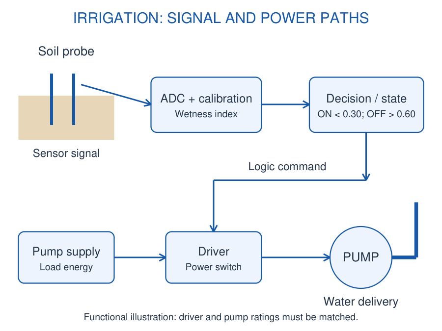
Functional workflow: Probe → conditioning/ADC → calibration → threshold plus state → output command → driver → pump. The microcontroller carries information; the pump obtains energy through a suitable power circuit. Add independent handling of dry-run, empty-tank or invalid-sensor conditions where the stated system requires them.
A dry/wet endpoint index is not automatically volumetric water content. Soil type, salinity, placement and sensor condition influence the reading. Record calibration conditions, and avoid comparing uncalibrated raw codes from different probes as if they were identical physical moisture values.
Fault reasoning: A disconnected sensor may imitate an endpoint. The algorithm should recognise its declared fault conditions and choose a defined response. Never infer that a real irrigation system is reliable from a single successful threshold example.
Worked Problem 4.46: Irrigation Hysteresis
Problem: Pump initially OFF. Turn ON below index 0.30 and OFF above 0.60. At other values retain state. Apply indices 0.50, 0.25, 0.45, 0.65, 0.40. Find commands.
Model / approach: Update state only at the specified threshold crossings.
Step 1: 0.50: stays OFF; 0.25: turns ON.
Step 2: 0.45: stays ON; 0.65: turns OFF; 0.40: stays OFF.
Answer: OFF, ON, ON, OFF, OFF.
Check: The same intermediate index can have a different command after a different history.
41. [C] Digital Thermometer and Fermentation pH Display
A digital thermometer converts the sensing output into a numerical temperature and displays it with a unit. An analog temperature element uses conditioning and ADC conversion; a digital temperature device supplies encoded data through its specified interface. Both still need valid calibration and sensible update timing.
The displayed precision should match the useful resolution and accuracy. Round the final calibrated value for presentation, rather than repeatedly rounding intermediate measurements. A change from Celsius to Fahrenheit requires an explicit numerical conversion, not a change of the printed unit symbol alone.
Fermentation pH: A high-impedance electrode requires suitable buffering and calibration before numerical interpretation. A two-point calibration sets offset and slope over a declared range; temperature and electrode condition can affect the result.
A controller can acquire temperature and pH as separate channels and show both on an LCD. Store the unit, timestamp and channel identifier when logging. Label an invalid reading instead of displaying a misleading default as an actual process value.
Reading rule: Raw code → calibrated physical quantity → rounded display. Keep the measurement model separate from the display format. A pH value is dimensionless; temperature still needs °C or another declared unit.
Worked Problem 4.47: Thermometer Display Rounding
Problem: A calibrated temperature is 27.36 °C. Display one decimal place and convert the unrounded value to °F.
Model / approach: Round only the final displayed quantities.
Step 1: Celsius display rounds to 27.4 °C.
Step 2: F = (9/5)27.36 + 32 = 81.248 °F.
Answer: 27.4 °C; Fahrenheit display 81.2 °F at one decimal place.
Check: Changing units requires conversion before rounding.
42. [C] Data Logging: Readings Become a Record
Data logging stores measurements over time so that trends, excursions and process changes can be examined later. A useful record contains timestamp or sample index, channel identity, measured value, unit and validity/status as appropriate.
Sampling interval and record size determine storage demand. If recording begins at t = 0 and includes the endpoint T, an exactly divisible schedule gives N = T/Δt + 1 records. A different start/stop convention gives a different count; state the convention before calculating.
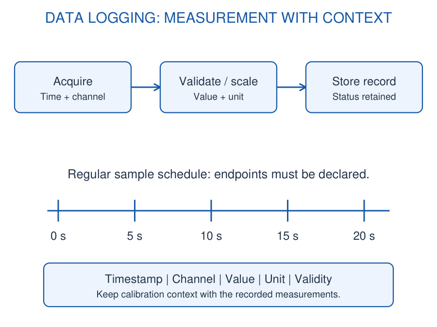
Storage bytes = number of records × bytes per record for a fixed-size binary format. Text files also require characters, separators and line endings, so a binary estimate should not be presented as an exact CSV file size. Distinguish bytes from bits and decimal kB from binary KiB.
Logging does not automatically imply cloud communication or real-time control. Data may be kept in local memory, removable storage or a computer through an appropriate interface. Loss of power, missing samples and invalid data must be handled by the chosen implementation.
Analysis example: Compare the temperature trend with fermentation pH changes or soil-moisture behaviour. Preserve timestamps and calibration information so that changes in the measurement setup are not mistaken for changes in the physical process.
Worked Problem 4.48: Binary Log Capacity
Problem: Each fixed-size record has a 4-byte timestamp, two 2-byte values and a 1-byte status. Find bytes for 3600 records. No header or padding.
Model / approach: Add fields before multiplying by record count.
Step 1: Record size = 4 + 2 + 2 + 1 = 9 bytes.
Step 2: Total = 3600 × 9 = 32400 bytes.
Answer: 32400 bytes = 32.4 decimal kB.
Check: This is the declared binary format, not an exact text-file estimate.
Worked Problem 4.49: Inclusive Sample Schedule
Problem: Record every 5 s from t = 0 through t = 60 s, both endpoints included. How many records?
Model / approach: List endpoints or use T/Δt + 1.
Step 1: 60/5 = 12 intervals.
Step 2: Including the initial sample gives 12 + 1.
Answer: 13 records.
Check: Starting at t = 5 s instead would give 12 records over the stated endpoint.
43. [C] Pulse-Oximeter Display: What the Number Means
A pulse oximeter uses optical sensing and processing to estimate arterial oxygen saturation and usually pulse rate. Red/infrared measurements, pulsatile components and a validated processing/calibration method contribute to the estimate; one arbitrary light intensity is not a complete SpO2 formula.
The display may show SpO2 in percent, pulse rate in beats per minute, a waveform or signal-quality indicator. A stored or invalid reading must not be presented as a current valid measurement. Motion, poor signal and measurement conditions can affect interpretation.
Functional chain: Optical sensing → analog conditioning → acquisition → validated processing → quality check → display. Unit IV focuses on representation and display; detailed instrument design belongs to a broader biomedical study.
Numerical display exercises below use an explicitly supplied processed value and scaling. They demonstrate decoding, units and rounding, not a clinical interpretation or an invented physiological algorithm.
Worked Problem 4.50: Processed Pulse-Oximeter Value
Problem: A teaching interface supplies a processed saturation integer 976 in units of 0.1% and pulse integer 72 in beats/min. Find the displayed values.
Model / approach: Decode the supplied engineering-unit representation.
Step 1: SpO2 = 976 × 0.1% = 97.6%.
Step 2: Pulse = 72 beats/min.
Answer: SpO2 97.6%; pulse 72 beats/min.
Check: These values are supplied processed data; no physiological estimate is derived from a raw light reading.
44. FORMULAE AND QUICK REVISION
| Quantity / Operation | Rule with Conditions |
|---|---|
| Unsigned N-bit range | 0 to 2^N – 1; 2^N patterns |
| Hex grouping | 1 hex digit corresponds to 4 bits |
| Noise margins | NMH = VOH,min – VIH,min; NML = VIL,max – VOL,max |
| De Morgan | (AB)’ = A’ + B’; (A + B)’ = A’B’ |
| Half adder | S = A XOR B; C = AB |
| Full adder | S = A XOR B XOR Cin; Cout = AB + Cin(A XOR B) |
| 2-to-1 MUX | Y = S’D0 + SD1 |
| Ideal unipolar ADC step | q = Vref/2^N; C = floor(Vin/q), range limited |
| Endpoint calibration | x = L + C(U – L)/(2^N – 1); declared mapping |
| Log storage | Bytes = record count × bytes per record |
Model check: State variable order, active level, clock event, code-transfer convention and units before choosing a rule. A steady-state truth table does not specify propagation delay or a complete physical interface.
QUICK REVISION: EXPLAIN AND CHECK
Why Is Binary Convenient?
Two defined logic states can be represented and regenerated despite bounded noise; their physical voltage ranges depend on the interface.
What Is the Difference Between 2^N and 2^N – 1?
The first is the number of N-bit patterns; the second is the largest unsigned index.
Does Boolean 1 + 1 Equal 2?
Boolean OR gives 1. Arithmetic addition gives binary 10 with a carry.
How Are De Morgan Complements Handled?
Change AND to OR or OR to AND and complement every operand while preserving the full scope.
Why Gray Order in a K-Map?
Neighbouring cells must differ in only one input bit, including valid wraparound edges.
Can a K-Map Group Contain Three Cells?
No. Use rectangular power-of-two groups; diagonal contact alone is not adjacency.
What Does a Don’t-Care Allow?
It may be used as 0 or 1 to simplify a care-row function. It never permits changing a required output.
How Do Half and Full Adders Differ?
A half adder adds two bits. A full adder also accepts an incoming carry.
What Does a MUX Do?
It copies the selected data input to the output under the declared enable/select conditions.
Why Does Stored State Require History?
The same present input may follow different earlier events and therefore coexist with different stored outputs.
What Does a D Flip-Flop Sample?
The D value at its active clock edge when setup/hold conditions are satisfied.
Is Every GPIO a Load-Power Output?
No. It supplies a limited logic command; significant loads require a suitable driver and power circuit.
Does More ADC Resolution Ensure Accuracy?
No. Reference, calibration, noise, offset and sensor error still matter.
Does a Ladder Contact Specify a Physical Safety Circuit?
No. It is a logical instruction; actual wiring and any required safety architecture are separate.
Why Log Units and Timestamps?
A number without measurement identity, time and calibration context can be misinterpreted.
Does a Pulse-Oximeter Display Derive Saturation?
The display presents processed data. A validated sensing and processing chain produces the estimate.
| Task | Core Operation | Essential Check |
|---|---|---|
| Boolean design | Truth table, laws and valid groups | All care rows retain their outputs |
| Arithmetic / routing | Carry weights or selected input | Declare width and control meaning |
| State storage | Hold or active-edge update | Initial state, setup and hold |
| Acquisition / display | Code, calibration and formatting | Reference, units and valid-data status |